S3F84B8_UM_REV 1.00 14 COMPARATOR
14-5
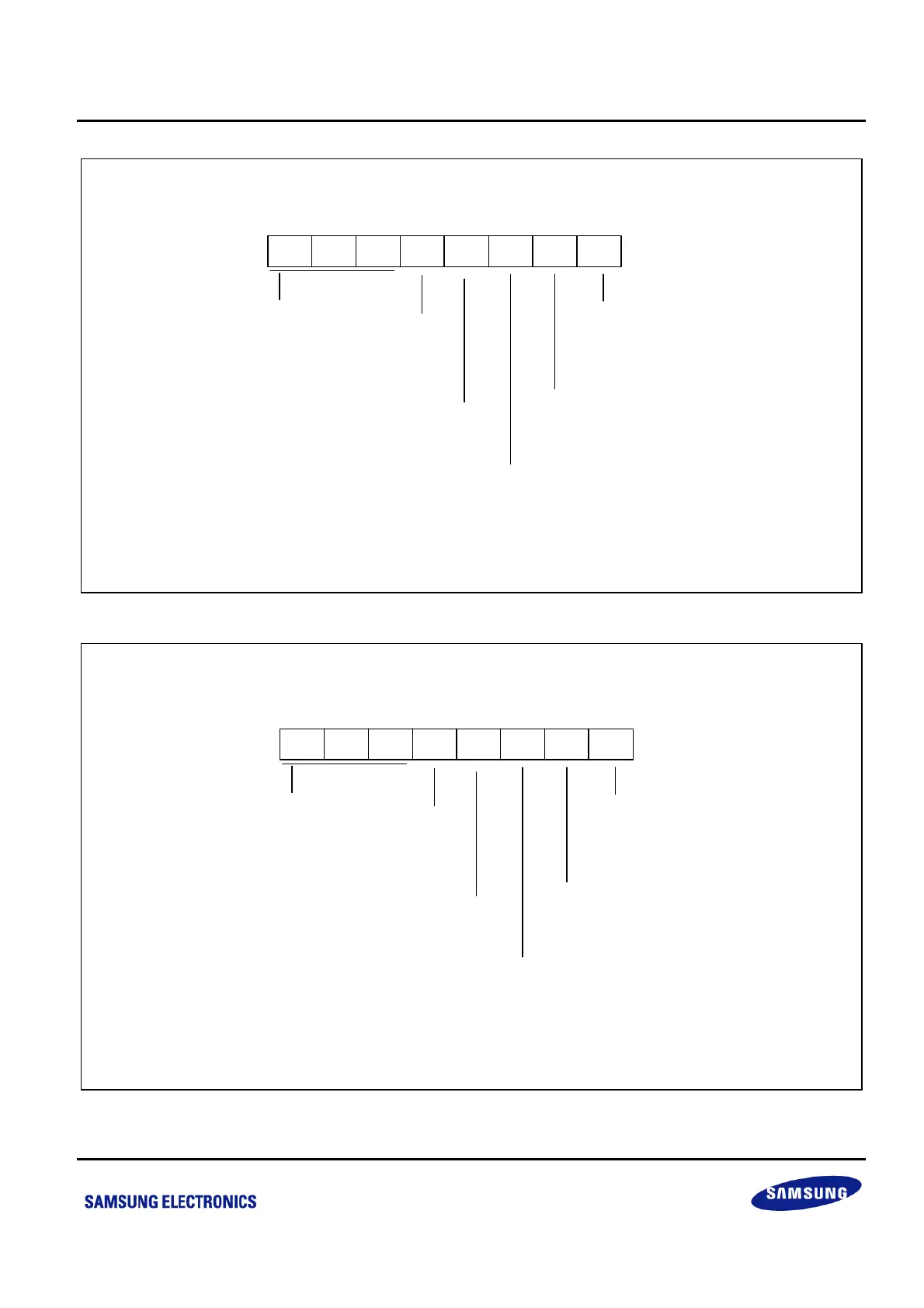
CMP1 Control Register (CMP1CON)
EBH, Set1, Bank0, Reset = 02H, R/W
.7 .6 .5 .4 .3 .2 .1 .0MSB LSB
CMP1 status bit
0 = CMP1_N > CMP1_P
1 = CMP1_N < CMP1_P
CMP 1 interrupt pending bit:
0 = No interrupt pending
(Clear pending bit when write)
1
= Interrupt is pending
CMP1 Interrupt enable bit
0 = Disable interrupt
1 = Enable interrupt
CMP 1 output polarity select bit
0 = CMP1 output is not inverted
1 = CMP1 output is inverted
CMP1 enable bit
0 = Disable comparator
1 = Enable comparator
CMP 1 reference level select bit
000 = 0.45VDD
001 = 0.50VDD
010 = 0.55VDD
011 = 0.60VDD
100 = 0.65VDD
101 = 0.70VDD
110 = 0.75VDD
111 = 0.80VDD
NOTE: Please refer to the programming tip for proper configuration sequence.
Figure 14-4 CMP1 Control Register (CMP1CON)
CMP2 Control Register (CMP2CON)
ECH, Set1, Bank0, Reset = 02H, R/W
.7 .6 .5 .4 .3 .2 .1 .0MSB LSB
CMP2 status bit
0=CMP2_N>CMP2_P
1=CMP2_N<CMP2_P
CMP 2 interrupt pending bit:
0 = No interrupt pending
(Clear pending bit when write)
1
= Interrupt is pending
CMP2 Interrupt enable bit
0 = Disable interrupt
1 = Enable interrupt
CMP 2 output polarity select bit
0 = CMP2 output is not inverted
1 = CMP2 output is inverted
CMP2 enable bit
0 = Disable comparator
1 = Enable comparator
CMP 2 reference level select bit
000 = 0.45VDD
001 = 0.50VDD
010 = 0.55VDD
011 = 0.60VDD
100 = 0.65VDD
101 = 0.70VDD
110 = 0.75VDD
111 = 0.80VDD
NOTE: Please refer to the programming tip for proper configuration sequence.
Figure 14-5 CMP2 Control Register (CMP2CON)