S3F84B8_UM_REV 1.00 14 COMPARATOR
14-7
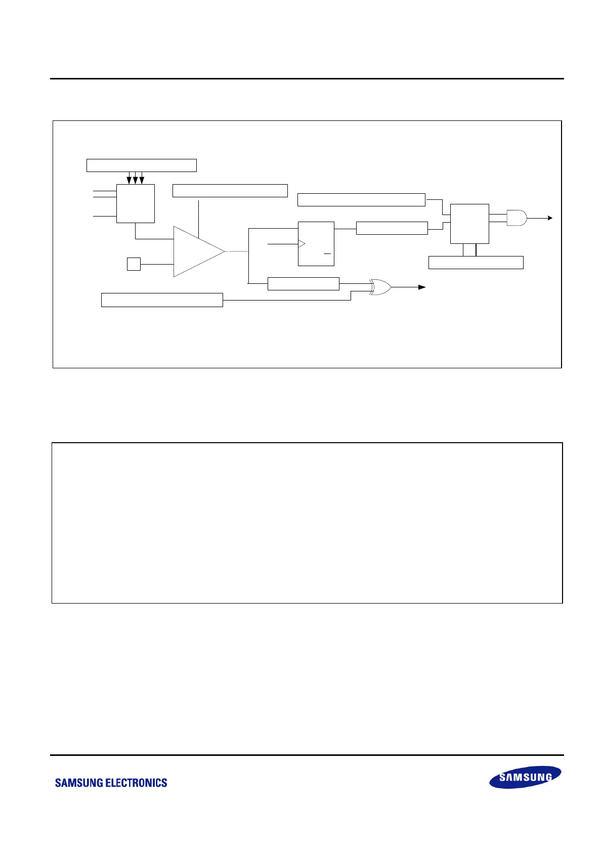
14.1.1.2.2 Block Diagram of Comparator 1/2/3
C1/2/3PLR (CMP1/2/3CON.4)
C1/2/3EN (CMP1/2/ 3CON.3)
PWM
CMP0_N
+
-
CMP1/2/3
Q
Q
SET
CLR
D
Interrupt
Fosc
CMP1/2/3CON.1
INT Enable (CMP1/2/3CON.2)
CMP1/2/3CON.7-.5
MUX
0.45 VDD
0. 50 VDD
0. 80 VDD
...
CMPINT.3-.2/.5-.4/.7-.6
INT
CTRL
CMP1/2/3CON.0
NOTE:
1. Polarity selection bit (CMP1/2/3CON.4) will not affect interrupt generation logic .
2. PWM lock signal is falling edge active only .
Figure 14-8 Block Diagram of Comparator 1/2/3
Example 14-1 Comparator Configuration
DI
LD CMPINT, #055H ; Falling edge interrupt
AND CMP0/1/2/3CON, #0FEH ; Must clear the pending bit before enabling CMP
LD CMP0/1/2/3CON, #0CH ; Enables CMP, enables interrupt
EI
 Loading...