S3F84B8_UM_REV 1.00 18 FLASH MCU ROM
18-2
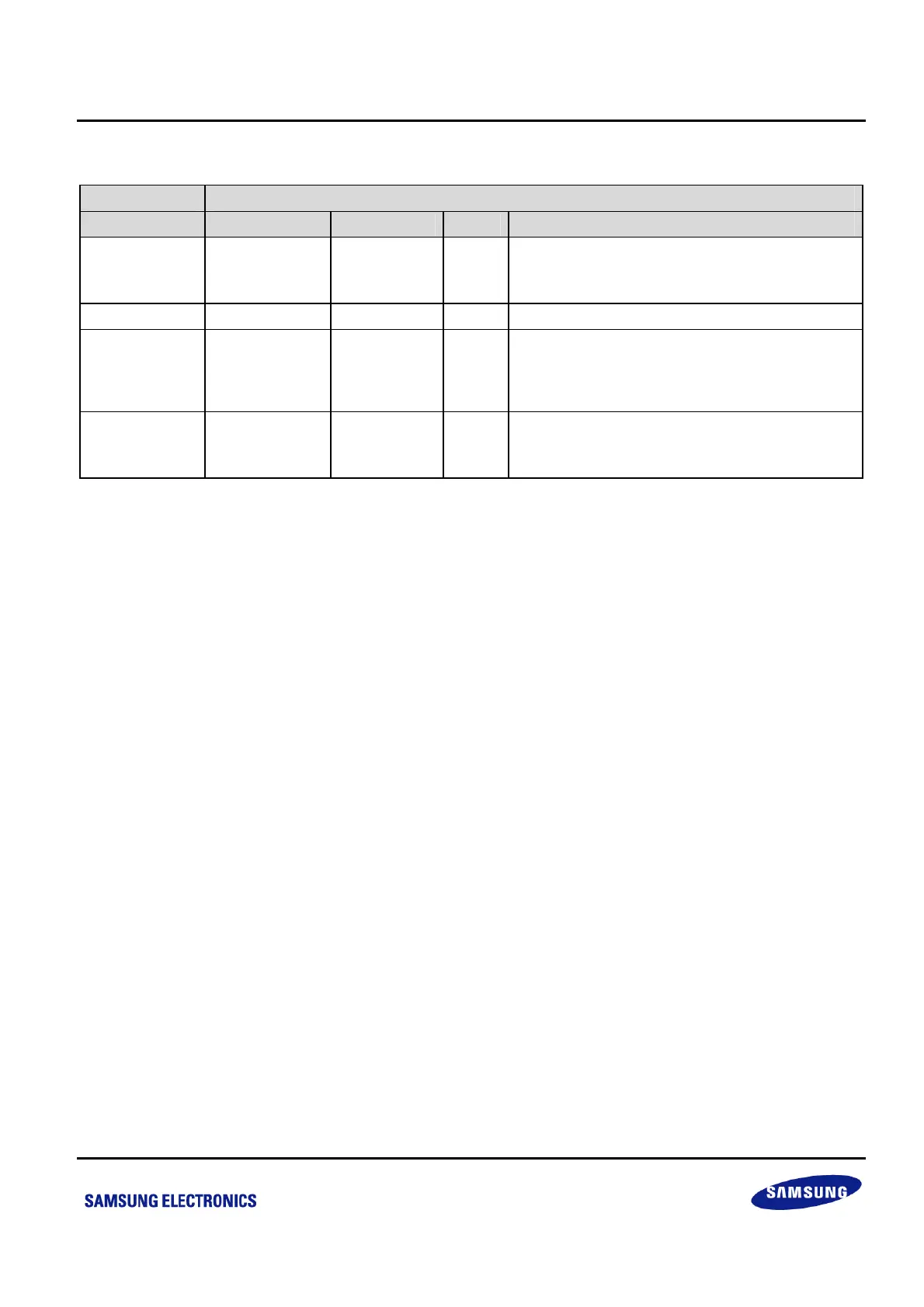
Table 18-1 Descriptions of Pins Used to Read/Write the Flash ROM
Main Chip During Programming
Pin Name Pin Name Pin Number I/O Function
P2.6
SDAT 18 I/O Serial data pin.
Specifies the output port while reading and input
port while writing.
P2.7 SCLK 19 I Serial clock pin.
RESET/P0.2 VPP 4 I Power supply pin for Flash ROM Cell Writing.
Using this pin, the MTP can enter into the writing
mode. If 11 V is applied, the MTP enters into the
Tool Program mode.
V
DD
, V
SS
V
DD
, V
SS
20,
1
– Power supply pin for logic circuit.
VDD should be tied to +5.0V during
programming.
NOTE: Vpp Pin Voltage
The Vpp pin on socket board for OTP/MTP writer should be 11V. Therefore, this pin must not be directly
connected to Vpp (12.5V) generated from some OTP/MTP writer. A specific adapter board for S3F84B8 must be
used while using these OTP/MTP writers.
 Loading...