CPU Architecture
2-3Central Processing Unit
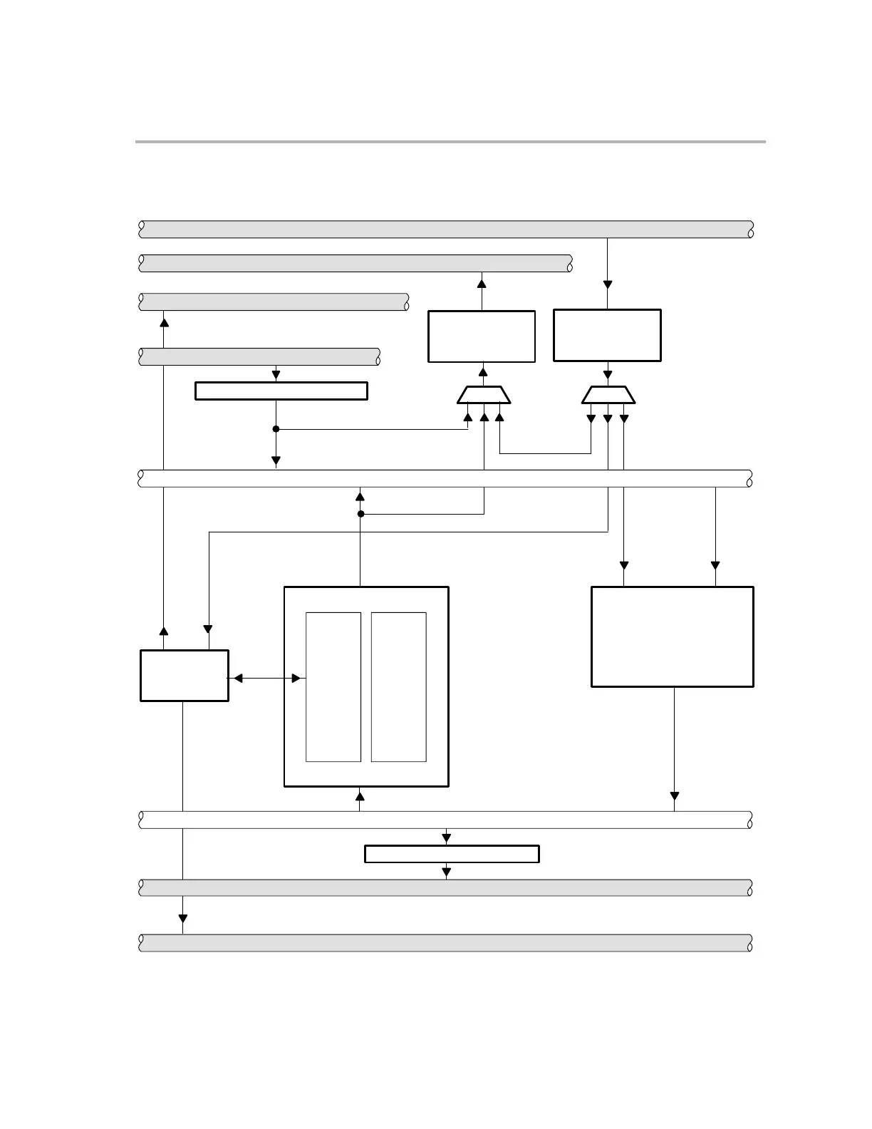
Figure 2−1. Conceptual Block Diagram of the CPU
Data-write buffer register
Immediate
data
XAR7
XAR0
XAR1
XAR2
XAR3
XAR4
XAR5
XAR6
XAR7
DP
SP
ST1
ARAU
Program-read data bus, PRDB(0:31)
Program address bus, PAB(0:21)
RESULT BUS
Data-read address bus, DRAB(0:31)
Data-read data bus, DRDB(0:31)
Data-read buffer register
Multiplier,
barrel shifter,
and
ALU
Data-/program-write data bus, DWDB(0:31)
Data-write address bus, DWAB(0:31)
Program-address
generation logic
Program control
logic
MUX
Immediate
address
Immediate
data
MUX
Address
from stack
AH:AL
PH:PL
T:TL
IER
DBGIER
IFR
ST0
PC
RPC
Result bus
Registers
Operand bus