Architecture Changes
F-7Migration From C27x to C28x
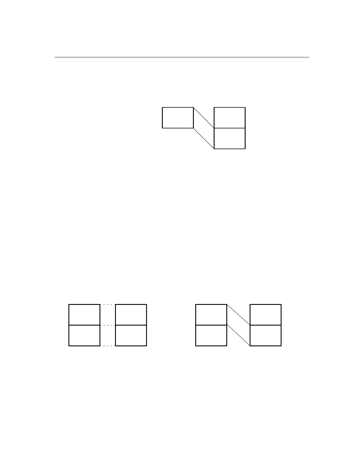
Figure F−4. Mapping of Memory Blocks B0 and B1 on C27x
B0 B1
B0
C27x
Program Space
Data Space
00 0000
00 0400
00 07FF
On a C28x device at reset, these blocks are mapped uniformly in both program
and data space as shown in Figure F−5. This can cause issues when running
C27x object code that relies on the C27x mapping. If your code relies on this
mapping, you can flip-block M0 and M1 in program space only by clearing the
M0M1MAP bit in status register 1 (ST1) to a 0. Executing the ”C27MAP” (or
”CLRC M0M1MAP”) instruction is the only way to clear this bit. With
M0M1MAP == 0, the mapping is compatible with the C27x B0 and B1 blocks
as shown in Figure D-4. Remember that after a reset M0 and M1 revert to the
C28x mapping.
It is strongly recommended that you migrate your code to use the default C28x
mapping of these blocks and not rely on the compatible mapping.
Figure F−5. C27x Compatible Mapping of Blocks M0 and M1
M0 M0
M1
C28 at Reset
(M0M1MAP = 1)
Program Space
Data Space
00 0000
00 0400
00 07FF
C27x Compatible Mapping
(M0M1MAP = 0)
M1 M0
M1
Program Space
Data Space
00 0000
00 0400
00 07FF
M0M1