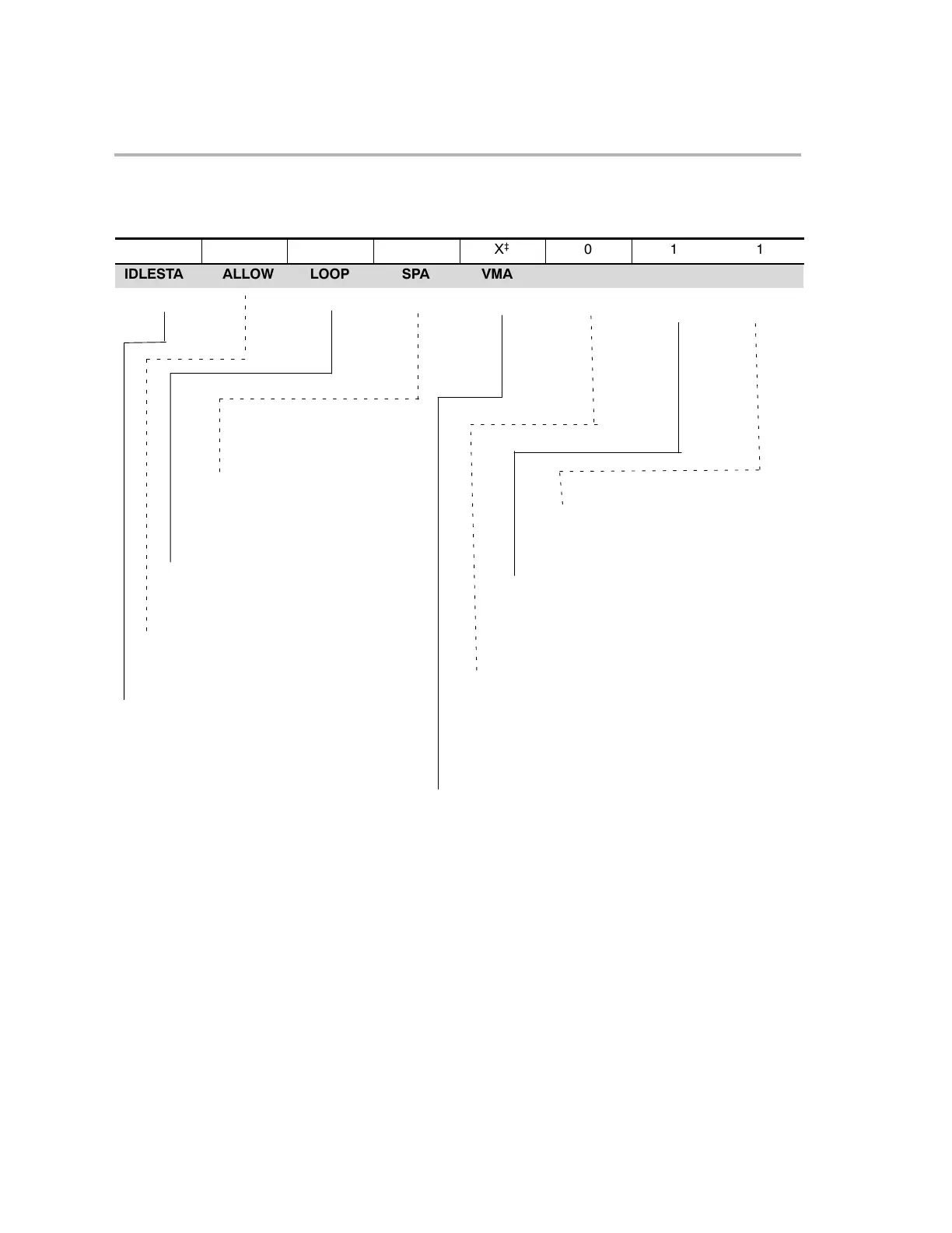
Register Figures
Figure A−3. Status Register ST1, Bits 7−0
76543210
0 0 0 0
ÉÉ
X
‡
ÉÉÉ
0 1 1
IDLESTAT EALLOW LOOP SPA VMAP PAGE0 DBGM INTM
R/W
R/W
Access to emulation registers disabled
Access to emulation registers enabled
0
1
Emulation access enable bit
R/W
R/WR/W
R/W
R
LOOPNZ/LOOPZ instruction done
LOOPNZ/LOOPZ instruction in
progress
0
1
Loop instruction status bit
Maskable interrupts globally enabled
Maskable interrupts globally disabled
0
1
Interrupt enable mask bit
Debug events enabled
Debug events disabled
0
1
Debug enable mask bit
PAGE0 addressing configuration bit
PAGE0 stack addressing mode
PAGE0 direct addressing mode
0
1
Interrupt vectors mapped to program-
memory addresses 000000
16
−00003F
16
Interrupt vectors mapped to program-
memory addresses 3FFFC0
16
−3FFFFF
16
0
1
Vector map bit
Stack pointer has not been
aligned to even address
Stack pointer has been aligned to
even address
0
1
Stack pointer alignment bit
IDLE instruction done
IDLE instruction in progress
0
1
IDLE status flag bit
R
†
These reserved bits are always 0s and are not affected by writes.
‡
The VMAP bit depends on the level of the VMAP input signal at reset. If the VMAP signal is low, the VMAP bit is 0 after reset;
if the VMAP signal is high, the VMAP bit is 1 after reset. For C28x devices that do not pin out the VMAP signal, the signal is tied
high internal to the device.
Note: For more details about ST1, see section 2.4 on page 2-34.