Introduction to the TMS320F28x7x
TMS320F2837xD Microcontroller Workshop - Architecture Overview 1 - 3
Introduction to the TMS320F28x7x
The TMS320F37xD, TMS320F37xS, and TMS320F07x, collectively referred to as the
TMS320F28x7x or F28x7x, are device members of the C2000™ microcontroller (MCU) product
family. These devices are most commonly used within embedded control applications. Even
though the topics presented in this workshop are based on the TMS320F2837xD dual-core
device series, most all of the topics are fully applicable to the TMS320F2837xS and
TMS320F2807x single-core device series. The F2837xD dual-core MCU design is based on the
TI 32-bit C28x CPU architecture. Each core is identical with access to its own local RAM and
flash memory, as well as globally shared RAM memory. Sharing information between the two
CPU cores is accomplished with an Inter-Processor Communications (IPC) module. Additionally,
each core shares access to a common set of highly integrated analog and control peripherals,
providing a complete solution for demanding real-time high-performance signal processing
applications, such as digital power, industrial drives, inverters, and motor control.
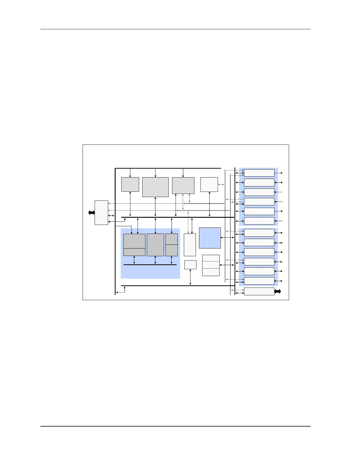
TMS320F28x7x Core Block Diagram
Sectored
Flash
Program Bus
Data Bus
RAM
Boot
ROM
3
32-bit
Timers
PIE
Interrupt
Manager
WD
CLA
CLA Bus
32x32 bit
Multiplier
FPU
CPU
Register Bus
R-M-W
Atomic
ALU
TMU
VCU
DMA
6 Ch.
DMA Bus
EMIF
ePWM
eCAP
eQEP
ADC
McBSP
I2C
SCI
SPI
CAN 2.0B
USB 2.0
GPIO
DAC
CMPSS
The above block diagram represents an overview of all device features and is not specific to any
one device. The F28x7x device is designed around a multibus architecture, also known as a
modified Harvard architecture. This can be seen in the block diagram by the separate program
bus and data bus, along with the link between the two buses. This type of architecture greatly
enhances the performance of the device.
In the upper left area of the block diagram is the memory section, which consists of the boot
ROM, sectored flash, and RAM. Also, notice that the six-channel DMA has its own set of buses.
In the lower left area of the block diagram is the execution section, which consists of a 32-bit by
32-bit hardware multiplier, a read-modify-write atomic ALU, a floating-point unit, a trigonometric
math unit, and a Viterbi complex math CRC unit. The control law accelerator (CLA) is an
independent and separate unit that has its own set of buses.
The peripherals are grouped on the right side of the block diagram. The upper set is the control
peripherals, which consists of the ePWM, eCAP, eQEP, and ADC. The lower set is the

 Loading...


