General Purpose Digital I/O
5 - 12 TMS320F2837xD Microcontroller Workshop - System Initialization
General Purpose Digital I/O
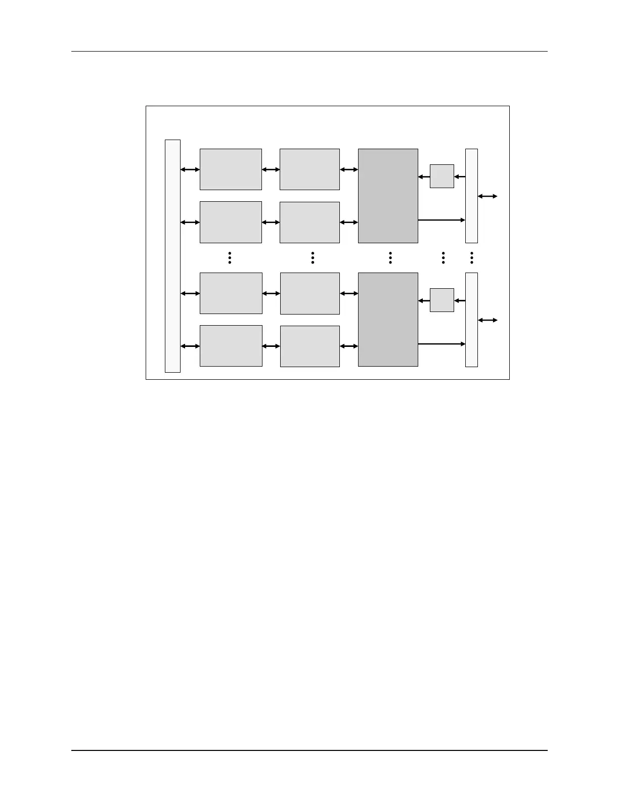
F28x7x GPIO Grouping Overview
Internal Bus
GPIO Port A Group
Mux1 Register
(GPAGMUX1)
[GPIO 0 to 15]
GPIO Port A
Direction Register
(GPADIR)
[GPIO 0 to 31]
GPIO Port A Mux1
Register
(GPAMUX1)
[GPIO 0 to 15]
GPIO Port A Group
Mux2 Register
(GPAGMUX2)
[GPIO 16 to 31]
GPIO Port A Mux2
Register
(GPAMUX2)
[GPIO 16 to 31]
GPIO Port A
Input
Qual
GPIO Port F Group
Mux1 Register
(GPFGMUX1)
[GPIO 160 to 175]
GPIO Port F
Direction Register
(GPFDIR)
[GPIO 160 to 191]
GPIO Port F Mux1
Register
(GPFMUX1)
[GPIO 160 to 175]
GPIO Port F Group
Mux2 Register
(GPFGMUX2)
[GPIO 176 to 191]
GPIO Port F Mux2
Register
(GPFMUX2)
[GPIO 176 to 191]
GPIO Port F
Input
Qual
The F2837xD device incorporates a multiplexing scheme to enable each I/O pin to be configured
as a GPIO pin or one of several peripheral I/O signals. Sharing a pin across multiple functions
maximizes application flexibility while minimizing package size and cost. A GPIO Group
multiplexer and four GPIO Index multiplexers provide a double layer of multiplexing to allow up to
twelve independent peripheral signals and a digital I/O function to share a single pin. Each output
pin can be controlled by either a peripheral or CPU1, CPU1 CLA, CPU2, or CPU2 CLA.
However, the peripheral multiplexing and pin assignment can only be configured by CPU1. By
default, all of the pins are configured as GPIO, and when configured as a signal input pin, a
qualification sampling period can be specified to remove unwanted noise. Optionally, each pin
has an internal pullup resistor that can be enabled in order to keep the input pin in a known state
when no external signal is driving the pin. The I/O pins are grouped into six ports, and each port
has 32 pins except for the sixth port which has nine pins (i.e. the remaining I/O pins). For a
GPIO, each port has a series of registers that are used to control the value on the pins, and within
these registers each bit corresponds to one GPIO pin.
If the pin is configured as GPIO, a direction (DIR) register is used to specify the pin as either an
input or output. By default, all GPIO pins are inputs. The current state of a GPIO pin
corresponds to a bit value in a data (DAT) register, regardless if the pin is configured as GPIO or
a peripheral function. Writing to the DAT register bit field clears or sets the corresponding output
latch, and if the pin is configured as an output the pin will be driven either low or high. The state
of various GPIO output pins on the same port can be easily modified using the SET, CLEAR, and
TOGGLE registers. The advantage of using these registers is a single instruction can be used to
modify only the pins specified without disturbing the other pins. This also eliminates any timing
issues that may occur when writing directly to the data registers.

 Loading...


