Oscillator/PLL Clock Module
TMS320F2837xD Microcontroller Workshop - System Initialization 5 - 3
Oscillator/PLL Clock Module
F28x7x Oscillator / PLL Clock Module
* default
X2
XTAL OSC
X1
XTAL
XCLKIN
(X2 n.c.)
Internal
OSC 1
(10 MHz)
Internal
OSC 2
(10 MHz)
OSCCLKSRCSEL
110
101
101
011
010
001
000*
PLL
PLLCLK
OSCCLK
PLLSYSCLK
(PLL bypass)
SYSPLLMULT
MUX
1/n
SYSCLKDIV
OSC1CLK
OSC2CLK
EXTCLK
WDCLK
XCLKOUT
(GPIO 73)
1x
00*
01
1/n
AUXPLLCLK
XCLKOUTDIV
XCLKOUTSEL
CPU2.SYSCLK
CPU1.SYSCLK
PLLCLK
PLLSYSCLK
AUX
PLL
1/n
AUXPLLCLK
AUXOSCCLKSRCSEL
AUXPLLDIV
00*
01
10
AUXCLKIN (from GPIO)
AUXCLK
0*
1
SYSPLLCTL1
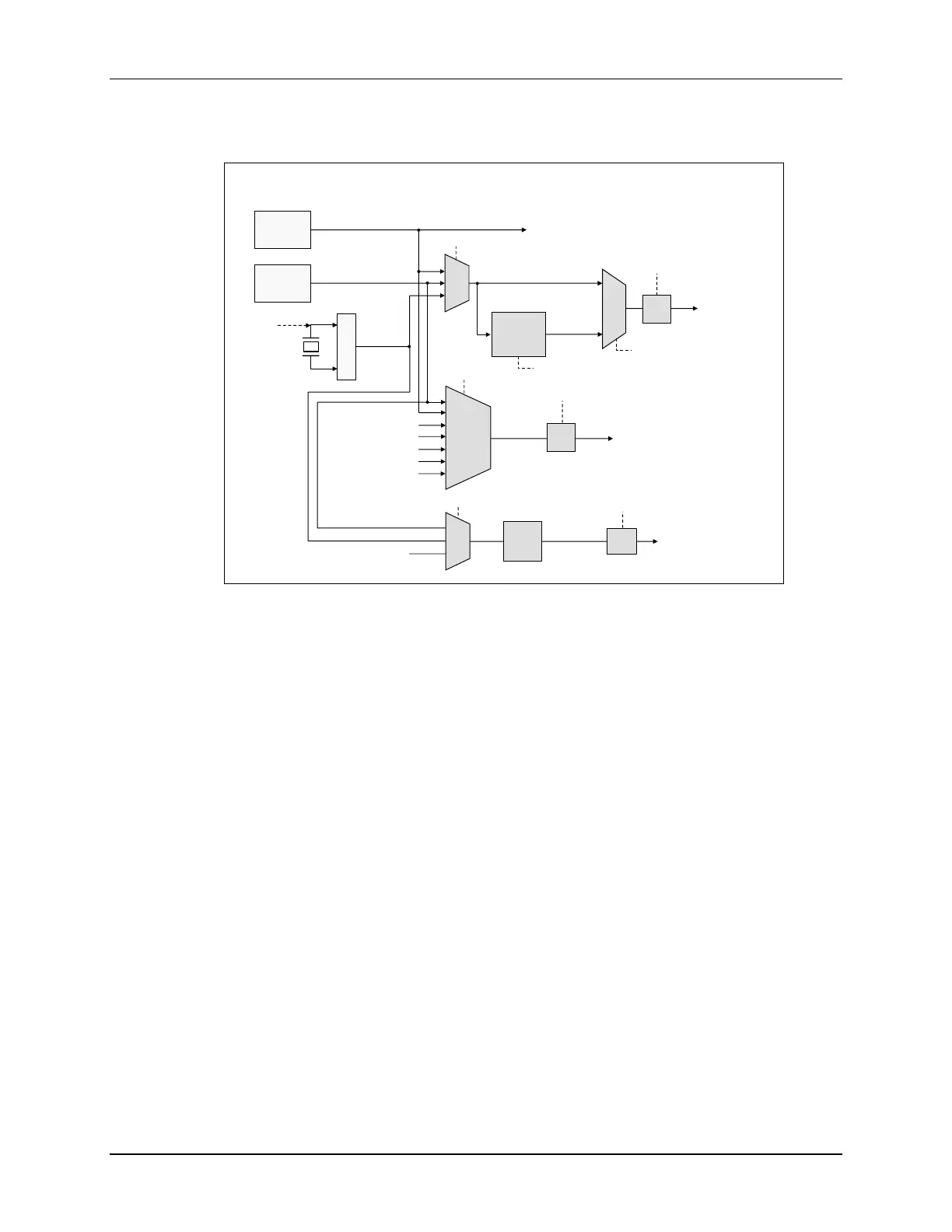
The device clock signals are derived from one of four clock sources: Internal Oscillator 1
(INTOSC1), Internal Oscillator 2 (INTOSC2), External Oscillator (XTAL), and Auxiliary Clock Input
(AUXCLKIN). At power-up, the device is clocked from the on-chip 10 MHz oscillator INTOSC2.
INTSOC2 is the primary internal clock source, and is the default system clock at reset. The
device also includes a redundant on-chip 10 MHz oscillator INTOSC1. INTOSC1 is a backup
clock source, which normally only clocks the watchdog timers and missing clock detection circuit.
Additionally, the device includes dedicated X1 and X2 pins for supporting an external clock
source such as an external oscillator, crystal, or resonator. The AUXCLKIN is used as the bit
clock source for the USB and CAN to generate the precise frequency requirements.

 Loading...


