Lab 8: Servicing the ADC with DMA
TMS320F2837xD Microcontroller Workshop - Direct Memory Access 8 - 15
Lab 8: Servicing the ADC with DMA
Objective
The objective of this lab exercise is to become familiar with operation of the DMA. In the previous
lab exercise, the CPU was used to store the ADC conversion result in the memory buffer during
the ADC ISR. In this lab exercise the DMA will be configured to transfer the results directly from
the ADC result registers to the memory buffer. ADC channel A0 will be buffered ping-pong style
with 50 samples per buffer. As an operational test, the 2 kHz, 25% duty cycle symmetric PWM
waveform (ePWM1A) will be displayed using the graphing feature of Code Composer Studio.
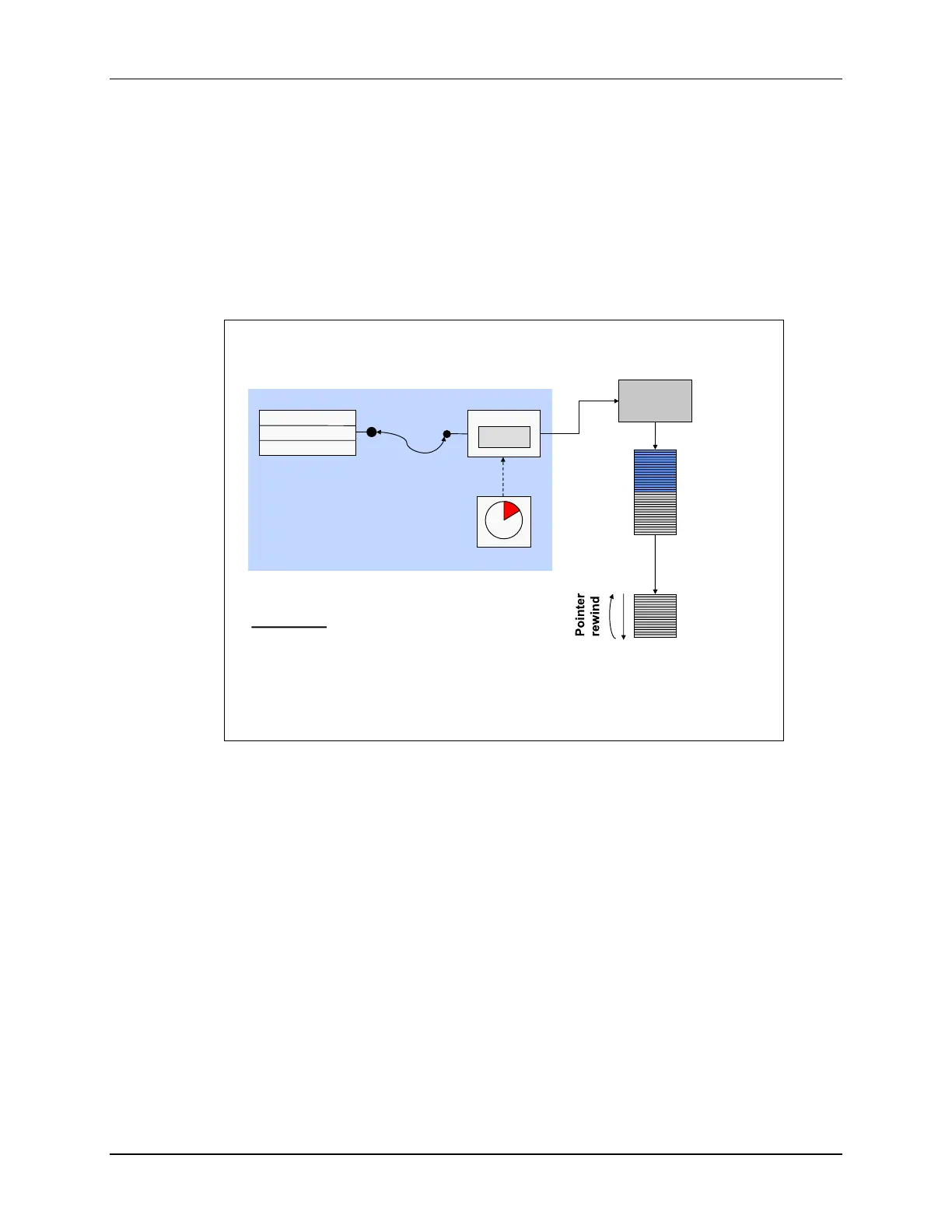
Lab 8: Servicing the ADC with DMA
ADC
RESULT0
ePWM2
jumper
wire
ADCINA0
data
memory
Display
using CCS
TB Counter
Compare
Action Qualifier
ePWM1
ePWM2 triggering ADC on period
match using SOCA trigger every
20 µs (50 kHz)
Objective:
Configure the DMA to buffer
ADCA Channel A0 ping-pong
style with 50 samples per buffer
ping
CPU writes data
to AdcBuf during
DMA ISR
pong
data
memory
DMA
Procedure
Open the Project
1. A project named Lab8 has been created for this lab exercise. Open the project by
clicking on Project Import CCS Projects. The “Import CCS Eclipse Projects”
window will open then click Browse… next to the “Select search-directory” box. Navigate
to: C:\C28x\Labs\Lab8\cpu01 and click OK. Then click Finish to import the project.
All build options have been configured the same as the previous lab exercise. The files
used in this lab exercise are:

 Loading...


