Reset and Boot Process
TMS320F2837xD Microcontroller Workshop - Reset and Interrupts 4 - 3
Reset and Boot Process
Reset Sources
POR – Power-on Reset generates a device reset during
power-up conditions
RESC – Reset Cause register contains the cause of the
last reset
(sticky bits maintain state with multiple resets)
Note: Only F2807x devices support an on-chip voltage regulator (VREG) to
generate the core voltage.
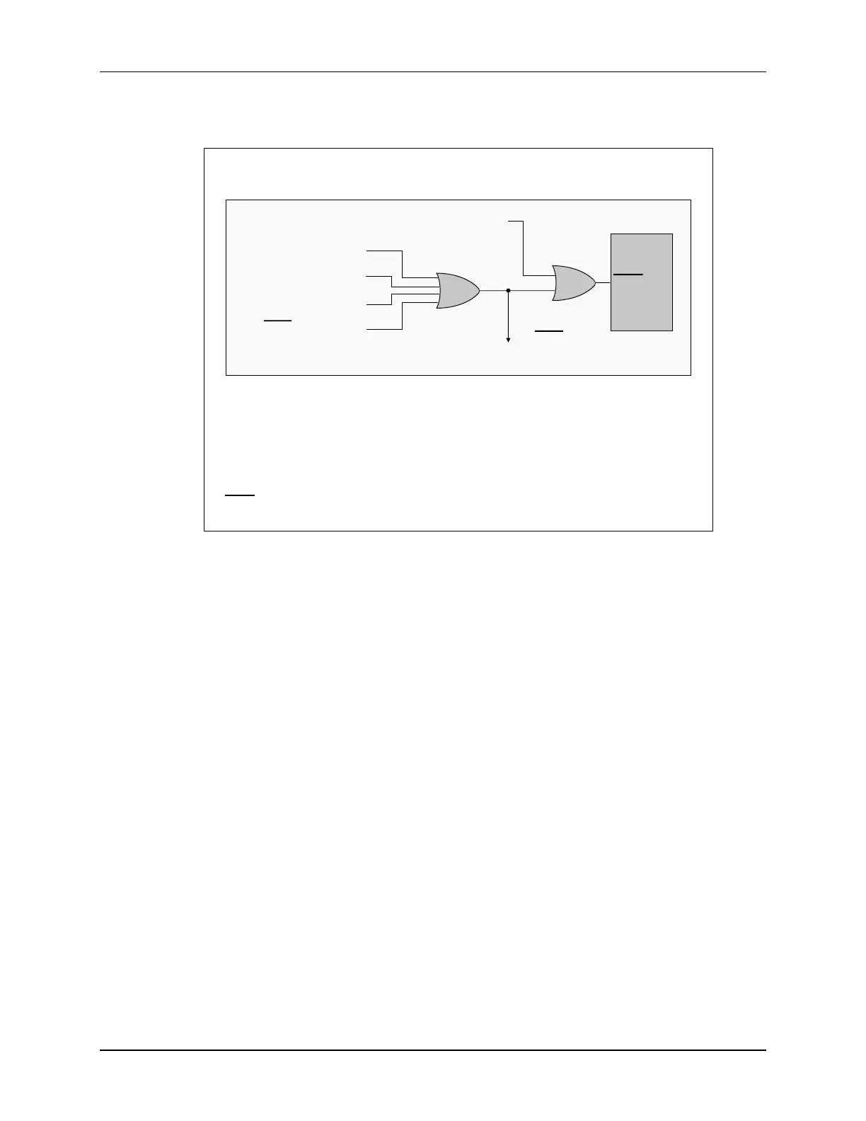
Watchdog Timer *
XRS pin active
To XRS pin
F28x7x
XRS
Power-on Reset
Hibernate Reset
Missing Clock Detect
Logic shown is functional representation, not actual implementation
* = CPU1.WD resets both cores and
CPU2.WD resets CPU2 only
The device has various reset sources, but in general resets on CPU1 will reset the entire device
and resets on CPU2 will reset only the CPU2 subsystem. The reset sources include an external
reset pin, watchdog timer reset, power-on reset which generates a device reset during power-up
conditions, Hibernate reset, as well as a missing clock detect reset. A reset cause register
(RESC) is available for each CPU subsystem which can be read to determine the cause of the
reset. The external reset pin is the main chip-level reset for the device, and it resets both CPU
subsystems to their default state. The power-on reset (POR) circuit is used to create a clean
reset throughout the device during power-up, while suppressing glitches on the input/output pins.
Note, only the F2807x devices support an on-chip voltage regulator to generate the core voltage.

 Loading...


