Lab 11: Inter-Processor Communications
TMS320F2837xD Microcontroller Workshop - Dual-Core Inter-Processor Communications 11 - 9
Lab 11: Inter-Processor Communications
Objective
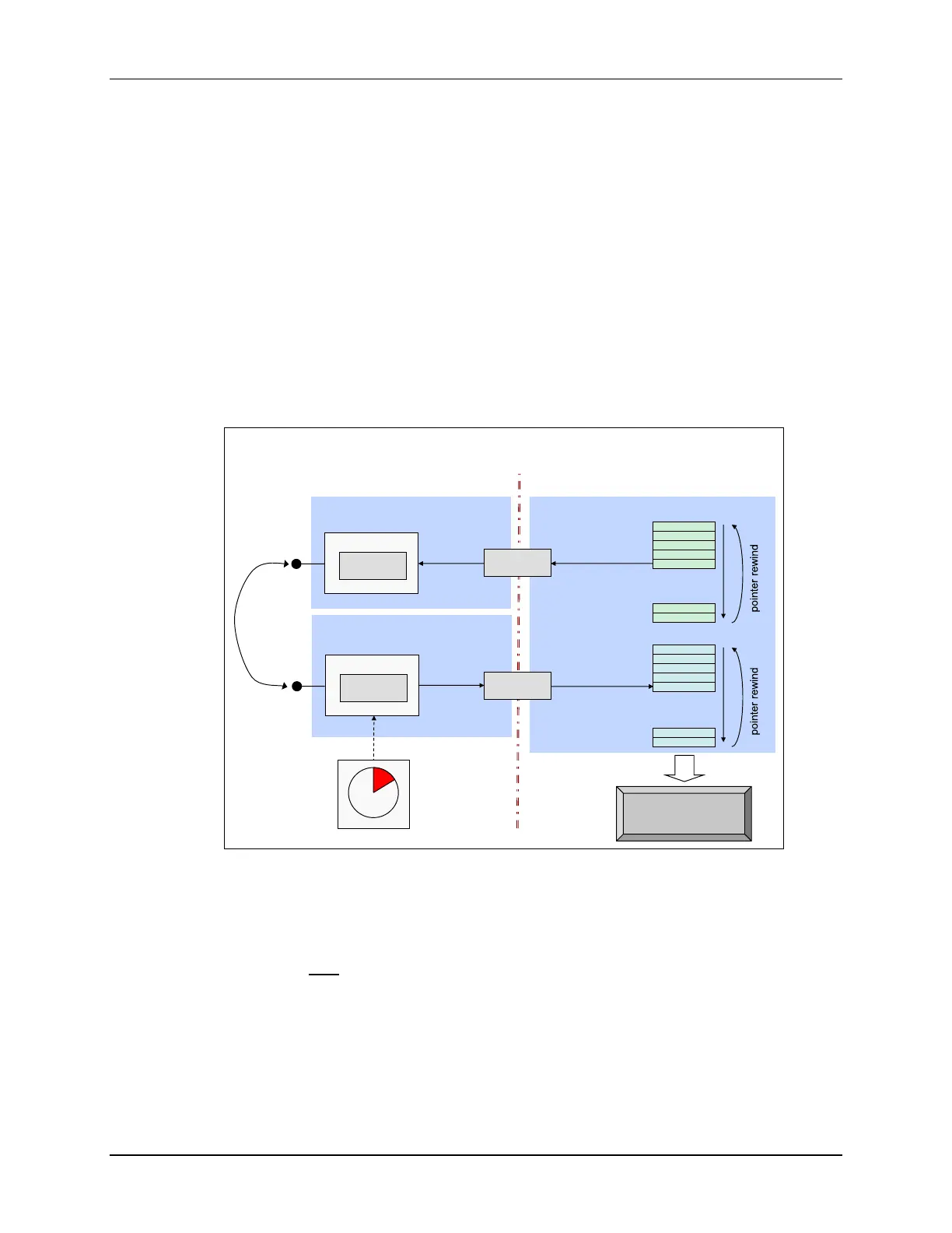
The objective of this lab exercise is to demonstrate and become familiar with the operation of the
IPC module. We will be using the basic IPC features to send data in both directions between
CPU1 and CPU2. A typical dual-core F2837xD application consists of two separate and
completely independent CCS projects. One project is for CPU1, and the other project is for
CPU2. As in the previous lab exercises, PWM2 will be configured to provide a 50 kHz SOC
signal to ADC-A. An End-of-Conversion ISR on CPU1 will read each result and write it into a
data register in the IPC. An IPC interrupt will then be triggered on CPU2 which fetches this data
and stores it in a circular buffer. The same ISR grabs a data point from a sine table and loads it
into a different IPC register for transmission to CPU1. This triggers an interrupt on CPU1 to fetch
the sine data and write it into DAC-B. The DAC-B output is connected by a jumper wire to the
ADCINA0 pin. If the program runs as expected, the sine table and ADC results buffer on CPU2
should contain very similar data.
Lab 11: Inter-Processor Communications
...
View ADC
buffer
Code Composer
Studio
PWM2 triggers
ADC-A at 50 kHz
...
jumper
wire
IPC1
IPC0
Sine Table
ADC Results
RESULT0
ADC-A
Pin 09
DACVALS
DAC-B
IPC1_ISR
1. Reads IPC1 data
and stores in circular
buffer
2. Writes next sine
data to IPC0
CPU1
CPU2
IPC0_ISR
Reads IPC0 data and writes into DAC-B
ADCA1_ISR
Reads ADC result and writes to IPC1
Pin 11
IPCRECVADDR
IPCSENDDATA
IPCSENDADDR
IPCRECVDATA
Toggle GPIO31 LED D10 @ 5 Hz
Toggle GPIO34 LED D9 @ 1 Hz
Procedure
Open the Projects – CPU1 & CPU2
1. Two projects named Lab11_cpu01 and Lab11_cpu02 have been created for this lab
exercise. Open both projects by clicking on Project Import CCS Projects. The
“Import CCS Eclipse Projects” window will open then click Browse… next to the “Select
search-directory” box. Navigate to: C:\C28x\Labs\Lab11 and click OK.
Both projects will appear in the “Discovered projects” window. Click Select All and click
Finish to import the project. All build options for each project have been configured the
same as the previous lab exercise.
The files used in the CPU1 project are:

 Loading...


