Introduction to the TMS320F28x7x
1 - 4 TMS320F2837xD Microcontroller Workshop - Architecture Overview
communication peripherals and consists of the multichannel buffered serial port, I2C, SCI, SPI,
CAN, and USB.
The PIE block, or Peripheral Interrupt Expansion block, manages the interrupts from the
peripherals. In the bottom right corner is the general-purpose I/O. The CPU has a watchdog
module and three 32-bit general-purpose timers are available. Also, the device features an
external memory interface, as shown on the left side.
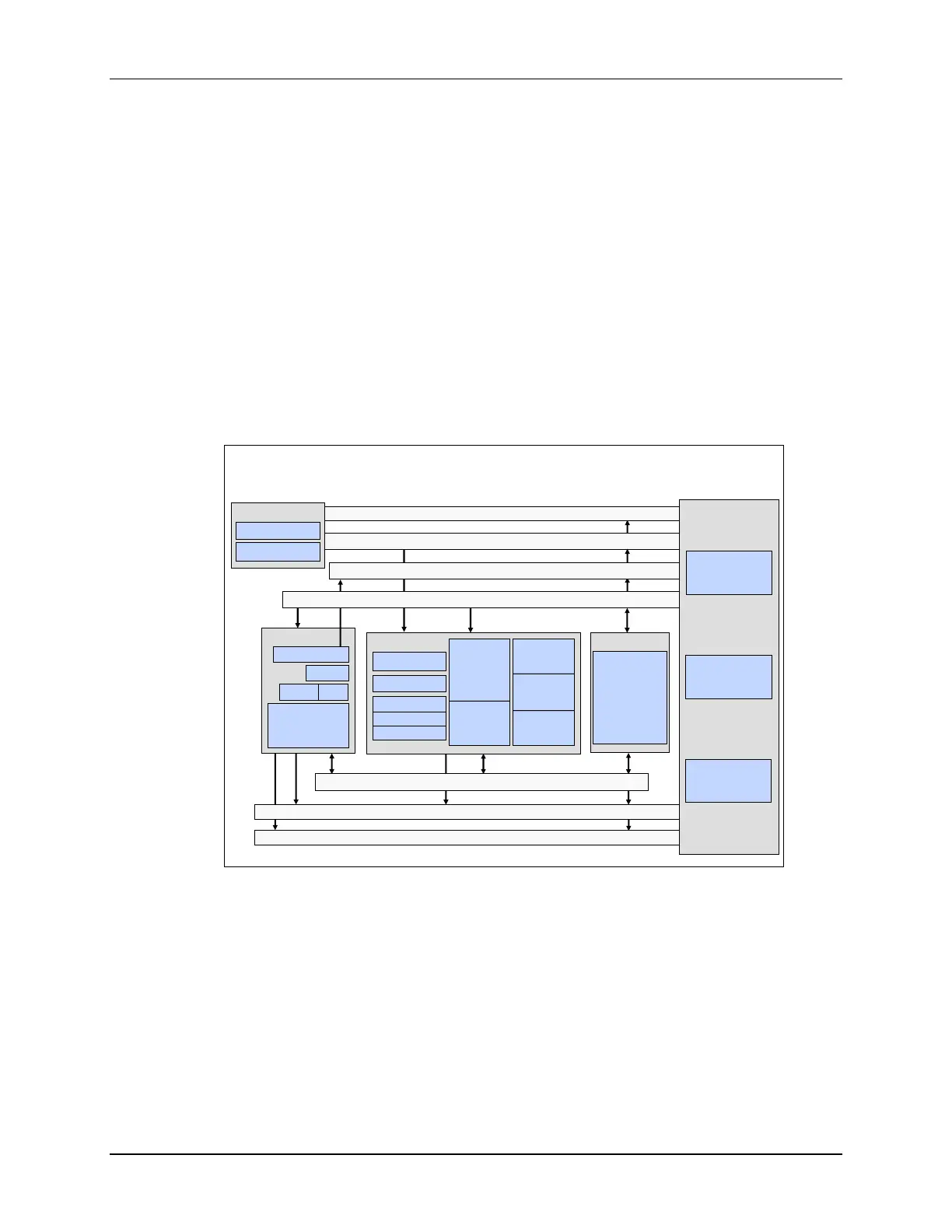
C28x Internal Bussing
As with many high performance microcontrollers, multiple busses are used to move data between
the memory blocks, peripherals, and the CPU. The C28x memory bus architecture consists of six
buses (three address and three data):
• A program read bus (22-bit address line and 32-bit data line)
• A data read bus (32-bit address line and 32-bit data line)
• A data write bus (32-bit address line and 32-bit data line)
Program-read Data Bus (32)
C28x CPU Internal Bus Structure
Data-write Address Bus (32)
Program Address Bus (22)
Execution
R-M-W
Atomic
ALU
Real-Time
JTAG
Emulation
Program
Decoder
PC
XAR0
to
XAR7
SP
DP @X
ARAU
MPY32x32
XT
P
ACC
ALU
Registers
Debug
Register Bus / Result Bus
Data/Program-write Data Bus (32)
Data-read Address Bus (32)
Data-read Data Bus (32)
TMU
TR0-TR7
Program
Memory
Data
Memory
Peripherals
VCU
VR0-VR8
CLA
MR0-MR3
FPU
R0H-R7H
The 32-bit-wide data busses provide single cycle 32-bit operations. This multiple bus architecture
(Harvard Bus Architecture) enables the C28x to fetch an instruction, read a data value and write a
data value in a single cycle. All peripherals and memory blocks are attached to the memory bus
with prioritized memory accesses.

 Loading...


