Memory
1 - 10 TMS320F2837xD Microcontroller Workshop - Architecture Overview
Memory
The F28x7x MCU utilizes a memory map where the unified memory blocks can be accessed in
either program space, data space, or both spaces. This type of memory map lends itself well for
supporting high-level programming languages. The memory structure consisting of dedicated
RAM blocks, shared local RAM blocks, shared global RAM blocks, message RAM blocks, Flash,
and one-time programmable (OTP) memory. The Boot is factory programmed with boot software
routines and standard tables used in math related algorithms.
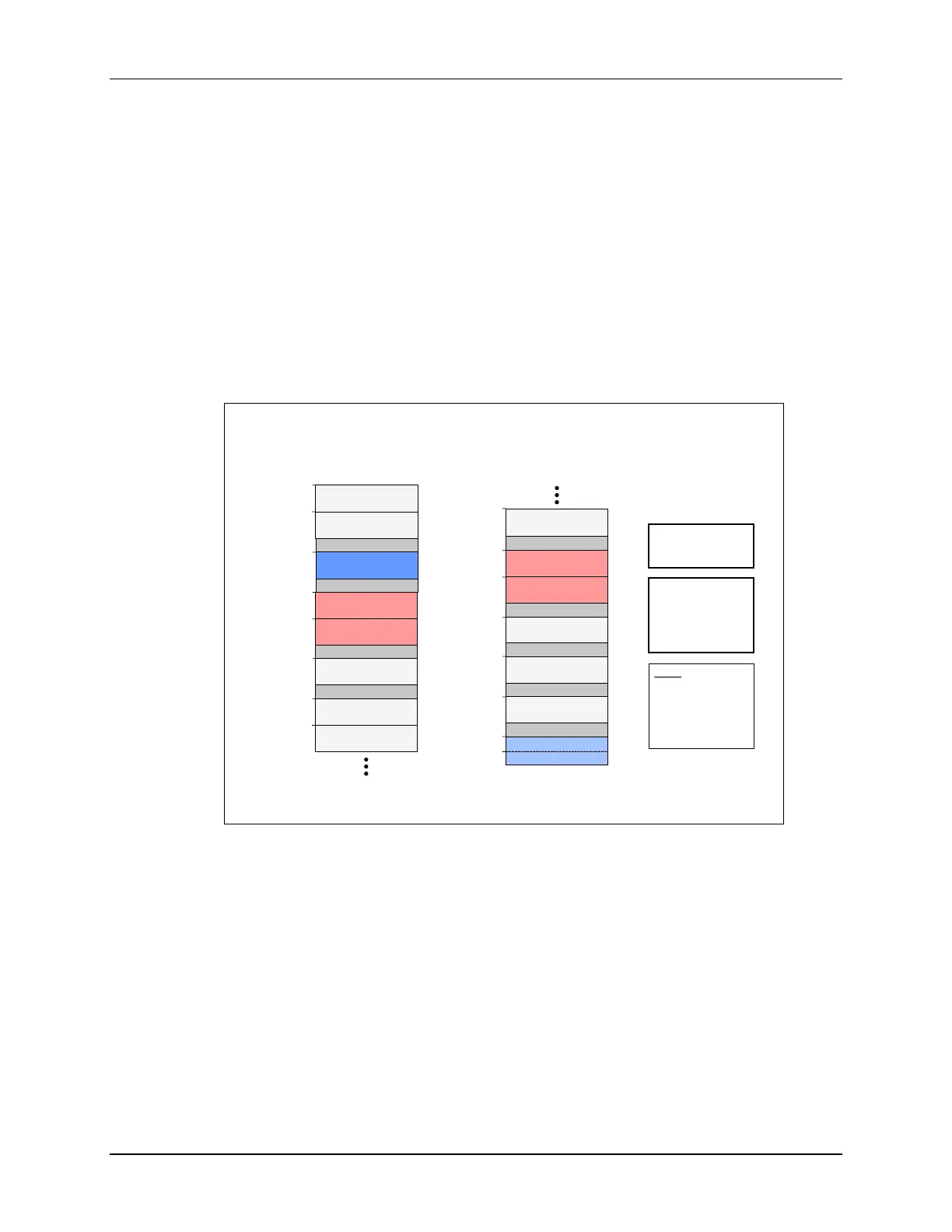
Memory Map
The C28x CPU core contains no memory, but can access on-chip and off-chip memory. The
C28x uses 32-bit data addresses and 22-bit program addresses. This allows for a total address
reach of 4G words (1 word = 16-bits) in data memory and 4M words in program memory.
Simplified F28x7x Memory Map
M0 RAM (1Kx16)
M1 RAM (1Kx16)
PIE Vectors
(512x16)
CLA to CPU MSG
RAM (128x16)
CPU to CLA MSG
RAM (128x16)
EMIF-2 (4Kx16)
LS0 - LS5 RAM
(2Kx16 each)
D0 - D1 RAM
(2Kx16 each)
0x000000
0x000400
0x000D00
0x001480
0x002000
0x008000
0x00B000
0x001500
GS0 - GS15 RAM
(4Kx16 each)
CPU2 to CPU1 IPC
MSG RAM (1Kx16)
CPU1 to CPU2 IPC
MSG RAM (1Kx16)
FLASH (256Kx16)
User OTP (1Kx16)
EMIF-1 (2Mx16)
Boot ROM
(32Kx16)
BROM Vectors (64x16)
0x00C000
0x03F800
0x03FC00
0x078000
0x080000
0x100000
0x3F8000
0x3FFFC0
LS0 - LS5 RAM
accessible by
CPU & CLA
GS0 - GS15
and EMIF1
accessible by DMA
(only GS0 - GS7
RAM on F2807x)
Notes:
1. Only EMIF-1 on
F2807x
2. IPC MSG RAMs
only on F2837xD
3. 512Kx16 FLASH
on F2837xS
There are four dedicated RAM block (M0, M1, D0, and D1) which are tightly coupled with the
CPU, and only the CPU has access to them. The PIE Vectors are a special memory area
containing the vectors for the peripheral interrupts. The six local shared memory blocks, LS0
through LS5, are accessible by its CPU and CLA. Global shared memory blocks GS0 through
GS15 on the F2837x and through GS7 on the F2807x are accessible by CPU and DMA.
There are two types of message RAM blocks: CPU message RAM blocks and CLA message
RAM blocks. The CPU message RAM blocks are used to share data between CPU1 subsystem
and CPU2 subsystem in a dual-core device via inter-processor communications. The CLA
message RAM blocks are used to share date between the CPU and CLA.
The user OTP is a one-time, programmable, memory block which contains device specific
calibration data for the ADC, internal oscillators, and buffered DACs, in addition to settings used
by the flash state machine for erase and program operations. Additionally, it contains locations
for programming security settings, such as passwords for selectively securing memory blocks,
configuring the standalone boot process, as well as selecting the boot-mode pins in case the

 Loading...


