External Memory Interface (EMIF)
10 - 6 TMS320F2837xD Microcontroller Workshop - System Design
Configurations for EMIF1 and EMIF2
Synchronous (SDRAM) Memory Support:
One, two, and four banks of SDRAMs
Devices with eight, nine, ten, and eleven column address
CAS latency of two or three clock cycles
Self-refresh and power-down modes
Asynchronous (SRAM and NOR Flash) Memory Support:
External “Wait” input for slower memories
Programmable read and write cycle timings: setup, hold, strobe
Programmable data bus width, and select strobe option
Extended Wait option with programmable timeout
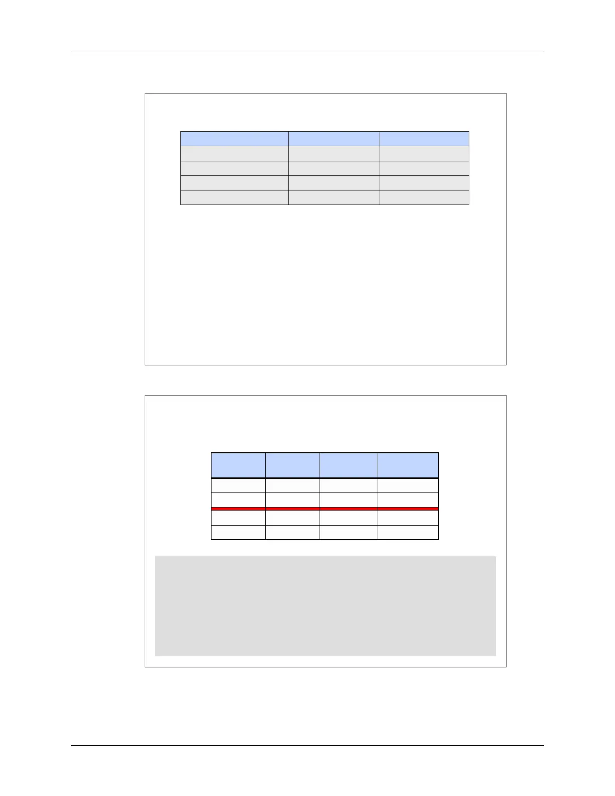
EMIF1 EMIF2
22-Bit (some pins muxed) 12-Bit
CSx Support 1 (CS0) 1 (CS0)
CSx Support 3 (CS2, CS3, CS4) 1 (CS2)
EMIF Performance
Notes: 1. A ‘word’ can be a 16- or 32-bit access
2. ASRAM assumed to have ta(A) of 10 or 12 ns (access time)
3. TMS320F2837x
a. ASRAM read setup/strobe/hold timings are 1/4/1, add 2 cycles bus start, 1 cycle data latency to CPU 9 cycles
(successive reads that are back-to-back do not incur the 1 cycle data latency, so 8*N+1 cycles for N “RPT” transfers)
b. ASRAM write setup/strobe/hold timings are 1/1/1, add 2 cycles bus start 5 cycles
c. ASRAM read assumes ta(OE) < 5 ns (This is typical for 10 or 12 ns ASRAM)
d. DRAM read, 100 MHz DRAM 14 cycles
e. DRAM write, 100 MHz DRAM 9 cycles
Memory
Type
Access
Type
CPU
Cycles
(Mword/s)
ASRAM read 9 22
DRAM read 14 14.3
ASRAM write 5 40
DRAM write 9 22.2
TMS320F2837x at 200 MHz SYSCLK

 Loading...


