APPENDIX
iKon-L APPENDIX
Page 154
If this is the first time you have used an Andor CCD, the glossary that follows will help familiarize you with its
design philosophy and some of its key terminology.
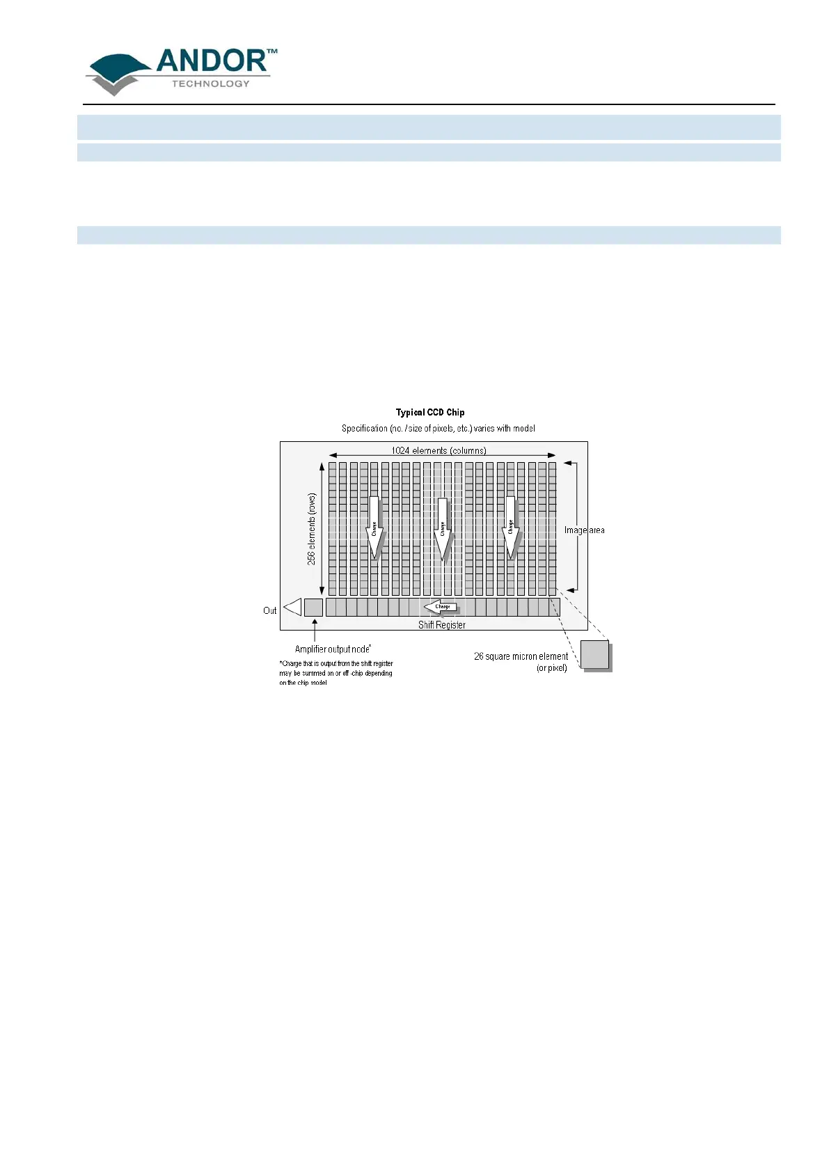
A Charge Coupled Device (or CCD) is a silicon-based semiconductor chip bearing a two-dimensional matrix of
photo-sensors, or pixels. This matrix is usually referred to as the image area. The pixels are often described as
being arranged in rows and columns (rows running horizontally, columns vertically). A typical CCD-chip may
comprise 400 rows and 1600 columns. The CCD in your detector is a scientific slow scan device (in contrast to
the fast scan CCD used in video cameras to capture moving images). An example of a typical layout is shown
here:
The Shift Register runs below and parallel to the light collecting rows. It has the same number of pixels as a
light-collecting row, but is itself masked, so that no light can fall on it. When light falls on an element, electrons
(photoelectrons) are produced and (in normal operation), these electrons are confined to their respective
elements. Thus, if an image (or any light pattern) is projected on to the array, a corresponding charge pattern
will be produced.
To capture the image pattern into computer memory, the charge pattern must be transferred off the chip, and
this is accomplished by making use of a series of horizontal (i.e. parallel to the rows/shift register) transparent
electrodes that cover the array. By suitable ‘clocking’, these electrodes can be used to shift (transfer) the entire
charge pattern, one row at a time, down into the shift register.
The shift register also has a series of electrodes (which are vertical, i.e. parallel to the columns) which are
used to transfer the charge packets, one element at a time, into the output node of the ‘on-chip’ amplifier.
The output of the amplifier feeds the analog-to-digital (A/D) converter, which in turn converts each charge
packet into a 16-bit binary number.
 Loading...