APPENDIX
iKon-L APPENDIX
Page 157
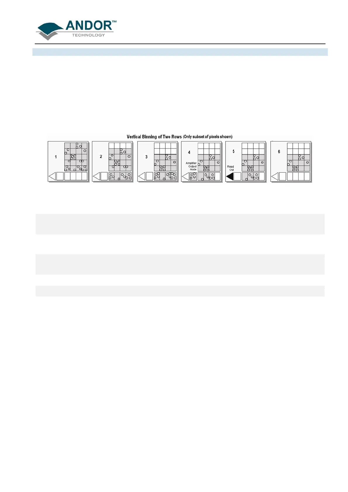
A1.1.6.1 - Vertical Binning
In Vertical Binning, charge from two or more rows of the CCD-chip is moved down into the shift register before
the charge is read out. The number of rows shifted depends on the binning pattern you have selected.
Thus, for each column of the CCD-chip, charge from two or more vertical elements is summed into the
corresponding element of the shift register. The charge from each of the pixels in the shift register is then
shifted horizontally to the output node of the amplifier and read out.
The figure below illustrates readout of data from adjacent tracks, each track comprising two binned rows of the
CCD-chip
:
Exposure to light causes a pattern of charge (an electronic image) to build up on the frame (or ‘image
area’) of the CCD-chip.
Charge in the frame is shifted vertically by one row, so that the bottom row of charge moves down into
the shift register.
Charge in the frame is shifted vertically by a further row, so that the next row of charge moves down into
the shift register, which now contains charge from two rows - i.e. the charge is vertically binned.
Charge in the shift register is moved horizontally by one pixel, so that charge on the endmost pixel of the
shift register is moved into the Gain Register
Charge is shifted into the output node of the amplifier
The charge in the output node of the amplifier is passed to the analog-to-digital converter and is read out
Steps 4 and 5 are repeated until the shift register is empty. The process is repeated from Step 2 until the
whole frame is read out
 Loading...