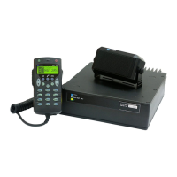
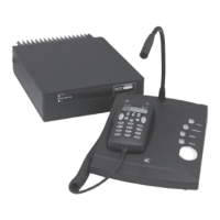
NGT—Technical description (2011/2012)
NGT Transceiver System Technical Service Manual 107
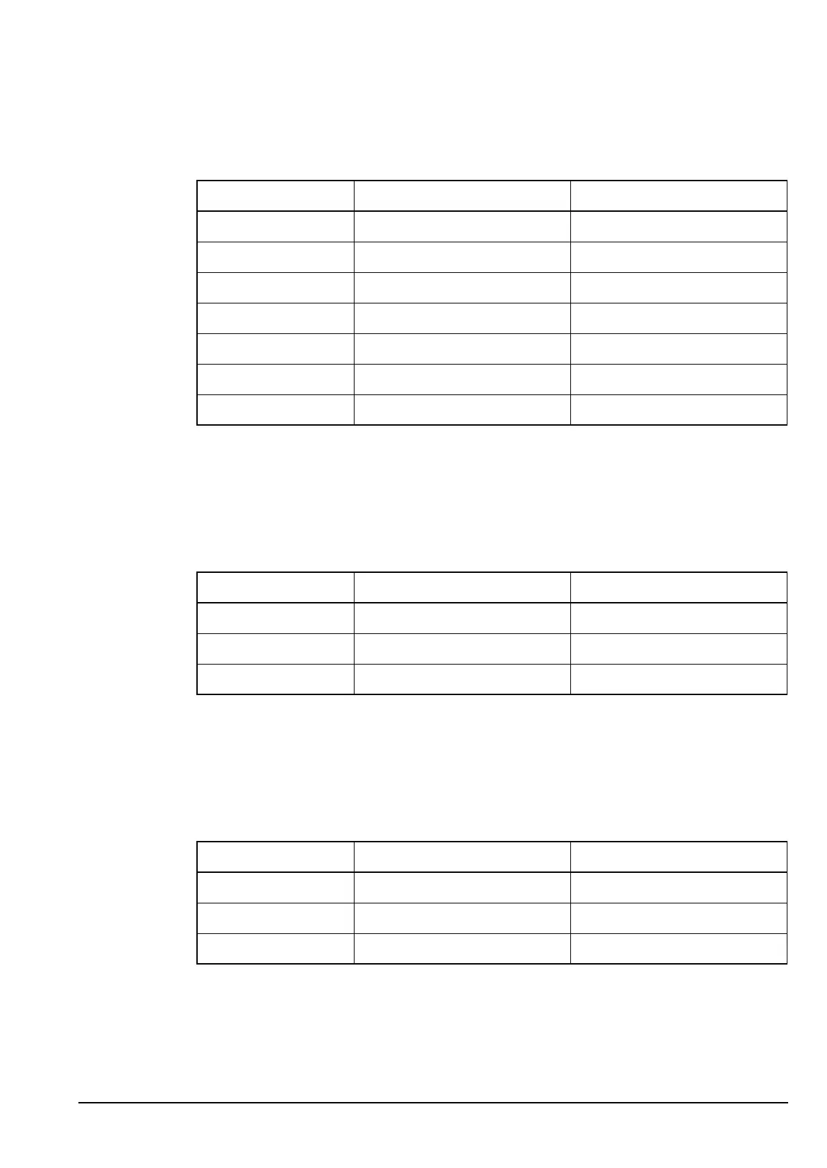
Drawings 04-03499 (sheet 1)
Table 28: Supply voltages for the Audio Interconnect & Data I/O PCB in the
RF unit (2012 only)
Supply Description Source
A Unregulated battery supply via Filter and Control PCB
A (protected) 2 A current-limited battery F1
+10 V +10 V regulated supply via Filter and Control PCB
+5 V +5 V regulated supply IC7
+2.5 VQ +2.5 V quiet for opamp bias IC7 (filtered)
+5 VQ +5 V quiet for opamp bias IC7 (filtered)
+5 VSBY +5.4 V standby for handset D3, D4
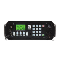
Drawings 04-03424 (sheet 1)
Table 29: Supply voltages for the Application Processor Handset I/F 3 V PCB
in the RF unit (2011 only)
Supply Description Source
+1V8 +1.8 V DSP core supply IC4
+3V3 +3.3 V switchmode supply IC5
+5 V +5 V regulated supply IC3
Drawings 04-03498 (sheet 1)
Table 30: Supply voltages for the Application Processor Handset & Data
I/F PCB in the RF unit (2012 only)
Supply Description Source
+1V8 +1.8 V DSP core supply IC4
+3V3 +3.3 V switchmode supply IC5
+5 V +5 V regulated supply IC3