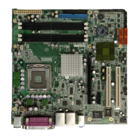
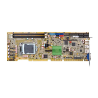
WSB-H810 PICMG 1.0 CPU Card
Page x
Figure 3-26: SPI Flash Connector Location...............................................................................42
Figure 3-27: SPI EC Flash Connector Location.........................................................................43
Figure 3-28: TPM Connector Location........................................................................................43
Figure 3-29: USB 2.0 Connector Pinout Locations ...................................................................44
Figure 3-30: USB 2.0 Connector (Type A) Pinout Location......................................................45
Figure 3-31: USB 3.0 Connector Location .................................................................................46
Figure 3-32: External Peripheral Interface Connector ..............................................................47
Figure 3-33: Ethernet Connector.................................................................................................47
Figure 3-34: VGA Connector .......................................................................................................49
Figure 4-1: Disengage the CPU Socket Load Lever..................................................................53
Figure 4-2: Remove Protective Cover.........................................................................................54
Figure 4-3: Insert the Socket LGA1150 CPU..............................................................................55
Figure 4-4: Close the Socket LGA1150 ......................................................................................55
Figure 4-5: Cooling Kit Support Bracket....................................................................................56
Figure 4-6: DIMM Installation.......................................................................................................57
Figure 4-7: Removing the Retention Screw and Standoff for a Half-size PCIe Mini Card.....58
Figure 4-8: Removing the Retention Screw...............................................................................59
Figure 4-9: Inserting the Full-size PCIe Mini Card into the Slot at an Angle..........................59
Figure 4-10: Securing the Full-size PCIe Mini Card ..................................................................60
Figure 4-11: Removing the Retention Screw.............................................................................61
Figure 4-12: Inserting the Half-size PCIe Mini Card into the Slot at an Angle........................61
Figure 4-13: Securing the Half-size PCIe Mini Card..................................................................62
Figure 4-14: Removing the Retention Screws...........................................................................63
Figure 4-15: Inserting the mSATA Card into the Slot at an Angle...........................................63
Figure 4-16: Securing the mSATA Card.....................................................................................64
Figure 4-17: AT/ATX Power Mode Switch Location ..................................................................64
Figure 4-18: Clear CMOS Button Location.................................................................................65
Figure 4-19: Flash Descriptor Security Override Jumper Location ........................................66
Figure 4-20: SATA Drive Cable Connection...............................................................................68
Figure 4-21: SATA Power Drive Connection..............................................................................69
Figure 6-1: Chipset Driver Welcome Screen........................................................................... 115
Figure 6-2: Chipset Driver License Agreement ...................................................................... 116
Figure 6-3: Chipset Driver Read Me File ................................................................................. 116
Figure 6-4: Chipset Driver Setup Progress............................................................................. 117
Figure 6-5: Chipset Driver Installation Finish Screen............................................................ 117
 Loading...