January 2007 73
Intel
®
855GME Chipset and Intel
®
6300ESB ICH Embedded Platform Design Guide
The signals below shall be isolated from the motherboard via specific termination resistors on the
ITP interposer itself according to interposer debug port recommendations. For the case where the
onboard ITP700FLEX debug port is used, refer to Section 4.3 for default termination
recommendations.
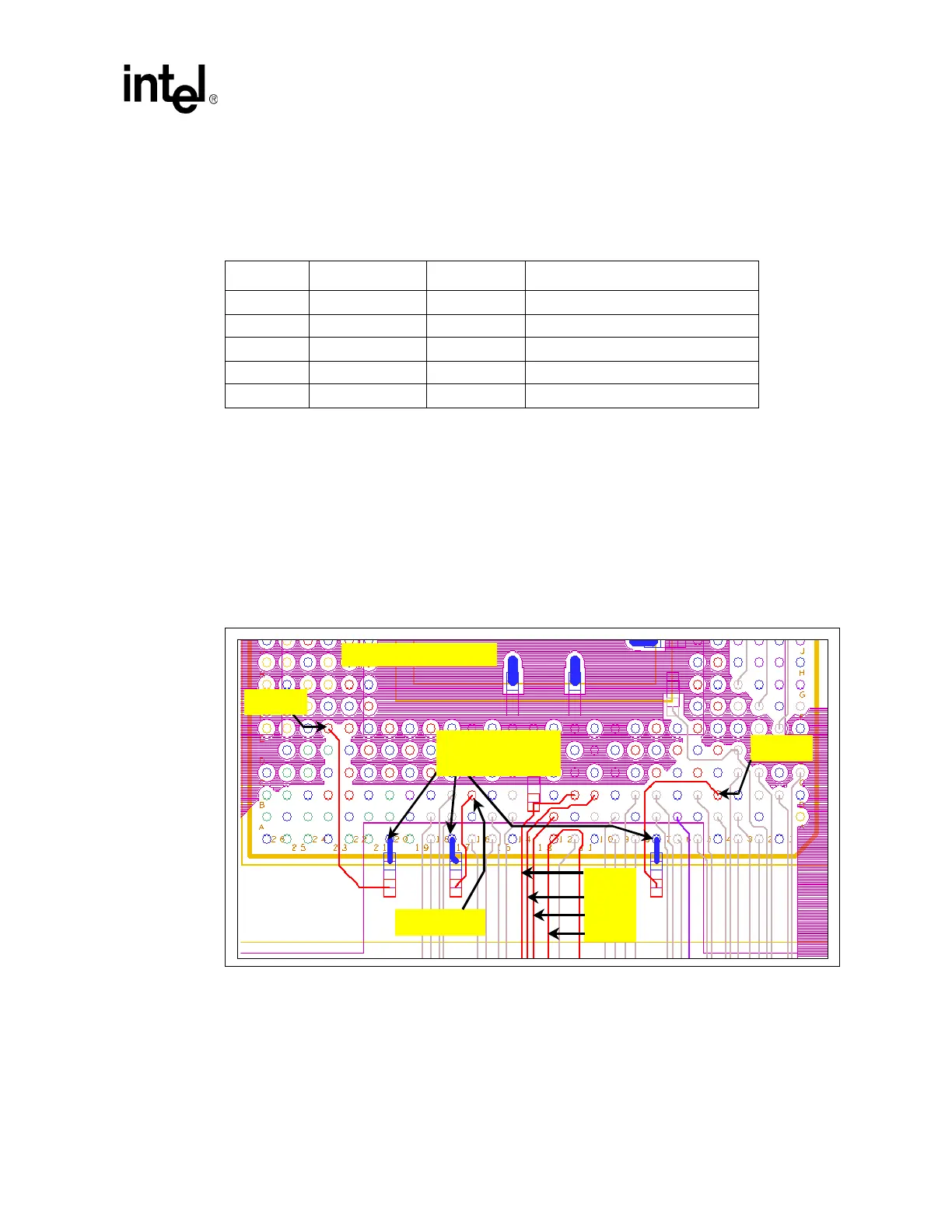
Figure 34 illustrates the recommended layout for the Intel Pentium M/Celeron M processor’s
strapping resistors. To avoid interaction with Intel Pentium M/Celeron M processor FSB routing,
the TEST[2:1] and RSVD (pin C16) signal resistors are placed on the secondary side of the
motherboard. To avoid GND via interaction with the Intel Pentium M/Celeron M processor FSB
routing, the resistors share GND via connections with the A8, A17, and A20 ground pins of the
Intel Pentium M/Celeron M processor.
The 150
Ω, pull-up resistor to V
CCP
(1.05 V) for TDI is shown in Figure 34 on the secondary side
of the board. The placement of the strapping resistors for TDI, TMS, TRST#, and TCK is not
critical.
Table 18. ITP Signal Default Strapping When ITP Debug Port Not Used
Signal Resistor Value Connect To Resistor Placement
TDI 150 Ω ± 5% VCCP Within 2.0” of the CPU
TMS 39
Ω ± 5% VCCP Within 2.0” of the CPU
TRST# 680
Ω ± 5% GND Within 2.0” of the CPU
TCK 27
Ω ± 5% GND Within 2.0” of the CPU
TDO Open NC N/A
Figure 34. Intel
®
Pentium
®
M/Celeron
®
M Processor Strapping Resistor Layout
SECONDARY SIDE
RSRVD C16
TDI
TMS
TRST#
TCK
TEST[2]
GND pins
TEST[1]