Development Capabilities and Interface
20-30 MPC823e REFERENCE MANUAL MOTOROLA
DEVELOPMENT
20
CAPABILITIES & INTERFACE
20.4.3.4 FREEZE. A freeze indication means that the processor is in debug mode and that
normal processor execution of user code is frozen. The freeze state is indicated on the FRZ
pin and is generated synchronous to the system clock. This indication can be used to halt
any off-chip device while in debug mode and is a handshake between the debug tool and
port. In addition to the FRZ pin, the freeze state is indicated by the value b11 on the VFLS
pins. The internal freeze status can also be monitored through status in the data shifted out
of the debug port.
20.4.3.5 DEVELOPMENT INTERFACE PORT REGISTERS. The development interface
port consists logically of three registers—development interface port instruction register,
development interface port data register, and trap enable control register. However, these
registers (DPIR/DPDR) are physically implemented as two registers—the development
interface port shift register and the trap enable control register (TECR). The development
interface port shift register acts as both the DPIR and DPDR, depending on the operation
being performed. It is also used as a temporary holding register for data to be stored in the
TECR. See Table 6-9 for more information and the DPIR and DPDR registers.
20.4.3.5.1 Development Interface Port Shift Register. The development interface port
shift register (DPIR/DPDR) is a 35-bit shift register. Instructions and data are serially shifted
into it from the DSDI using DSCK or CLKOUT as the shift clock, which depends on the
debug port clock mode. For more information, refer to Section 20.4.3.6 Development Port
Serial Communication.
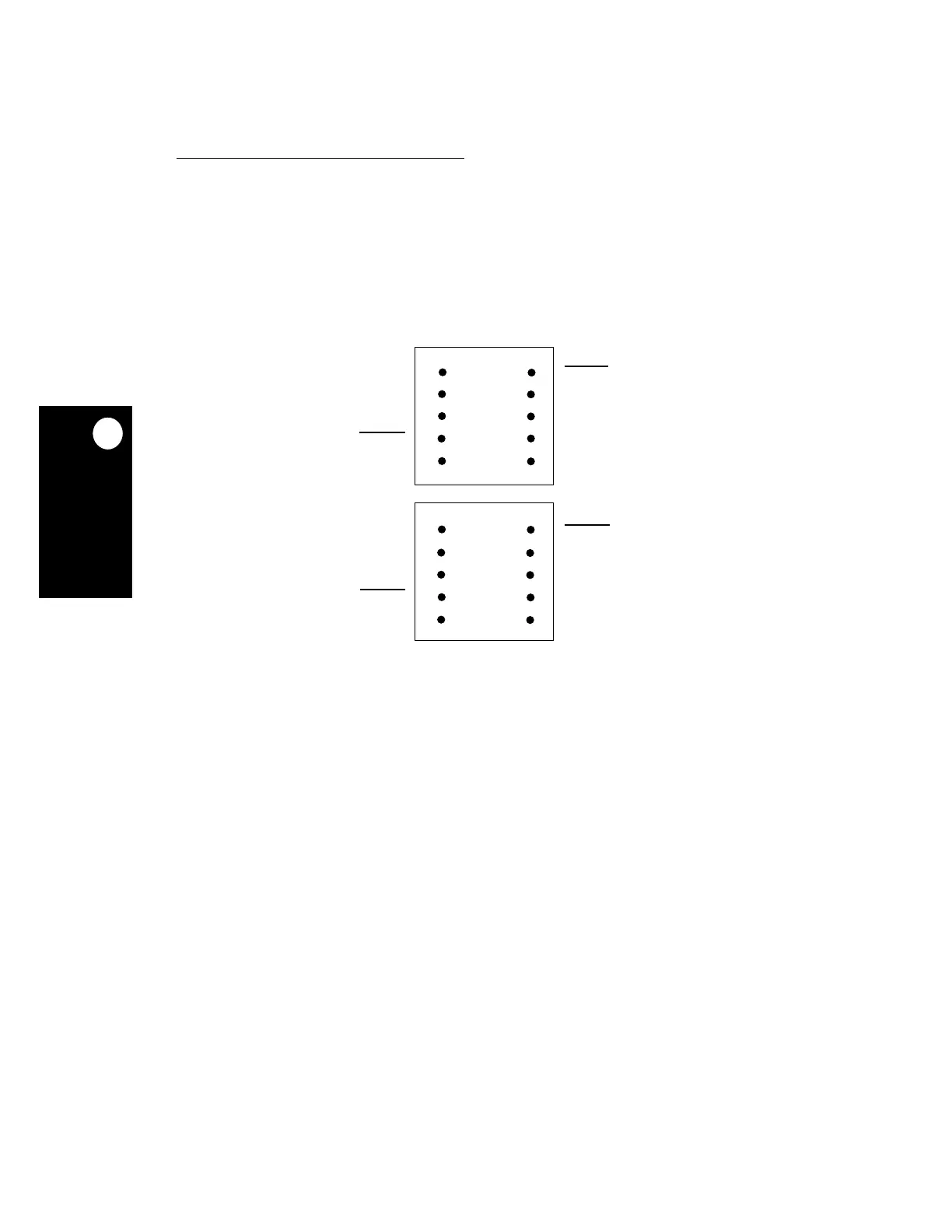
Figure 20-8. Development Port/Background Development Mode
Connector Pinout Options
12
3
4
56
78
910
12
3
4
56
78
910
VFLS0
GND
GND
HRESET
V
SRESET
DSCK
VFLS1
DSDI
DSDO
DD
FRZ
GND
GND
HRESET
V
SRESET
DSCK
FRZ
DSDI
DSDO
DD
 Loading...

