Memory Controller
MOTOROLA
MPC823e REFERENCE MANUAL
15-7
MEMORY CONTROLLER
15
15.3 REGISTER MODEL
The status bits for each one of the memory banks are in the memory controller status
(MSTAT) register, which is used by the entire memory controller. Each of the eight memory
banks has a base register (BRx) and an option register (ORx). The MSTAT reports write-
protect violations that occur and parity errors for every bank. The base register contains a V
bit that indicates when the information for the chip-select is valid.
Each base register defines the starting address of its memory bank and each option register
defines the attributes for its memory bank. The option registers also define the initial address
multiplexing for a memory cycle controlled by a UPM. The machine A mode register (MAMR)
and machine B mode register (MBMR) define most of the global features for the
user-programmable machines.
The memory command register (MCR) and memory data register (MDR) are used to
initialize the UPM’s RAM array. The MAD field of the memory command register specifies
the location in the RAM array to be executed as defined by the MCR. The memory address
register (MAR) allows a specific address pattern to be output onto the A[6:31] signals. The
memory periodic timer prescaler register (MPTPR) defines the divisor of the BRGCLK used
as the memory periodic timer input clock.
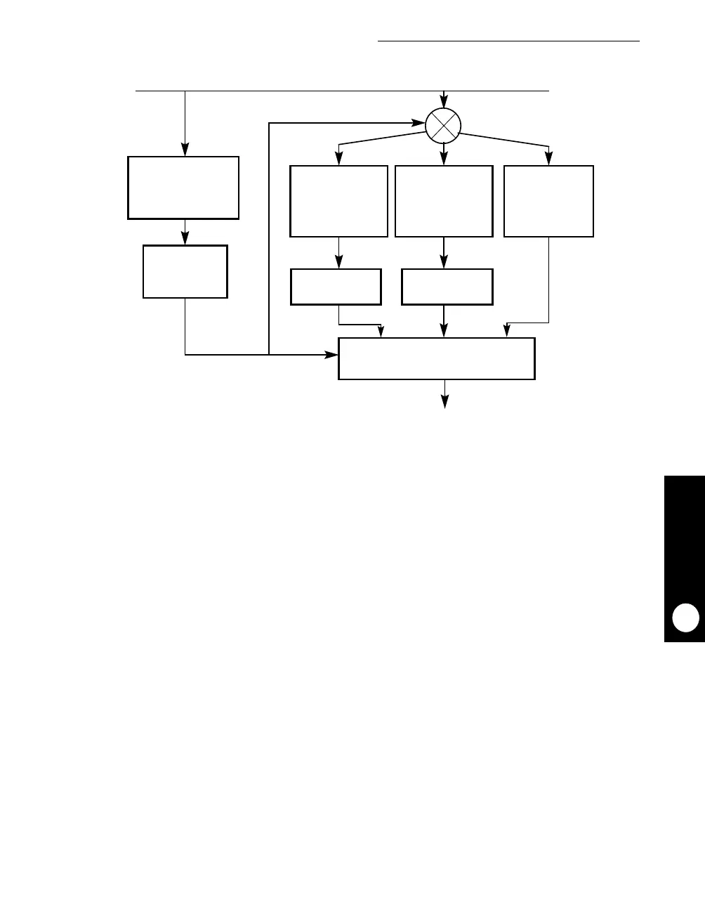
Figure 15-4. Basic Memory Controller Operation
SIGNALS
TIMING GENERATOR
INTERNAL/EXTERNAL MEMORY ACCESS REQUEST
PROGRAMMABLE
MACHINE A
GENERAL-PURPOSE
CHIP-SELECT
SIGNALS
TIMING GENERATOR
MS
ADDRESS COMPARATOR
BANK SELECT
MUX
EXTERNAL SIGNALS
ADDRESS,
USER-
PROGRAMMABLE
MACHINE B
USER-
MACHINE
FIELD
ADDRESS TYPE