Memory Management Unit
MOTOROLA MPC823e REFERENCE MANUAL 11-43
MEMORY MANAGEMENT
11
UNIT
UWP3—Problem (User) Write Permission Page Three
0 = Subpage 3 (address[20:21]=11) problem write access is not permitted.
1 = Subpage 3 (address[20:21]=11) problem write access is permitted.
11.6.3 MMU Instruction Content-Addressable Registers
The MI_CAM, MI_RAM0, and MI_RAM1 registers are interface registers that allow you to
read the data memory management unit CAM and RAM entries. If you try to write to the
MI_CAM register using the mtspr instruction, the CAM and RAM values of the entry indexed
by the DTLB_INDX field to MI_CAM, MI_RAM0, and MI_RAM1 will be loaded. The source
register in the mtspr instruction can be any register, since its value is not used. The values
of the MI_CAM, MI_RAM0, and MI_RAM1 registers can be read using the mfspr instruction.
If you try to write to the MI_RAM0 and MI_RAM1 registers using the mtspr instruction, it will
be considered a NOP (no operation) instruction.
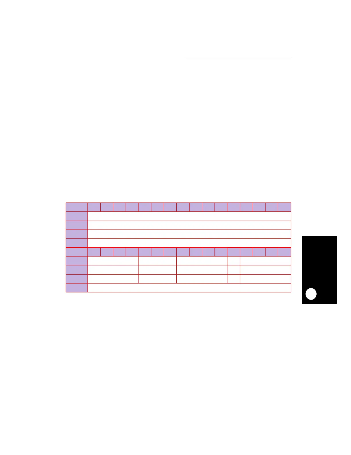
11.6.3.1 MMU INSTRUCTION CAM ENTRY READ REGISTER. When the
content-addressable memory of the MMU instruction CAM entry read (MI_CAM) register is
read, it contains the effective address and page sizes of an entry indexed by the ITLB_INDX
field of the MI_CTR. This register is only updated when you write a value to it.
EPN—Effective Page Number
These bits are the most-significant bits of the page’s effective address.
MI_CAM
BIT 0 1 2 3 4 5 6 7 8 9 10 11 12 13 14 15
FIELD EPN
RESET —
R/W R
ADDR SPR 816
BIT 16 17 18 19 20 21 22 23 24 25 26 27 28 29 30 31
FIELD EPN PS ASID SH SPV
RESET — — ———
R/W R R RRR
ADDR SPR 816
NOTE: — = Undefined.