Memory Management Unit
11-46 MPC823e REFERENCE MANUAL MOTOROLA
MEMORY MANAGEMENT
11
UNIT
SFP—Privileged (Supervisor) Fetch Permission
Bit 28:
0 = Subpage 0 (address[20:21]=00) privileged fetch is not permitted.
1 = Subpage 0 (address[20:21]=00) privileged fetch is permitted.
Bit 29:
0 = Subpage 1 (address[20:21]=01) privileged fetch is not permitted.
1 = Subpage 1 (address[20:21]=01) privileged fetch is permitted.
Bit 30:
0 = Subpage 2 (address[20:21]=10) privileged fetch is not permitted.
1 = Subpage 2 (address[20:21]=10) privileged fetch is permitted.
Bit 31:
0 = Subpage 3 (address[20:21]=11) privileged fetch is not permitted.
1 = Subpage 3 (address[20:21]=11) privileged fetch is permitted.
11.6.3.3 MMU INSTRUCTION RAM ENTRY READ REGISTER 1. The MMU instruction
RAM entry read register 1 (MI_RAM1) contains the protection mode information of the entry
indexed by the ITLB_INDX field of the MI_CTR. This register is only updated when you write
to the MI_CAM register.
Bits 0–25—Reserved
These bits are reserved and must be set to zero.
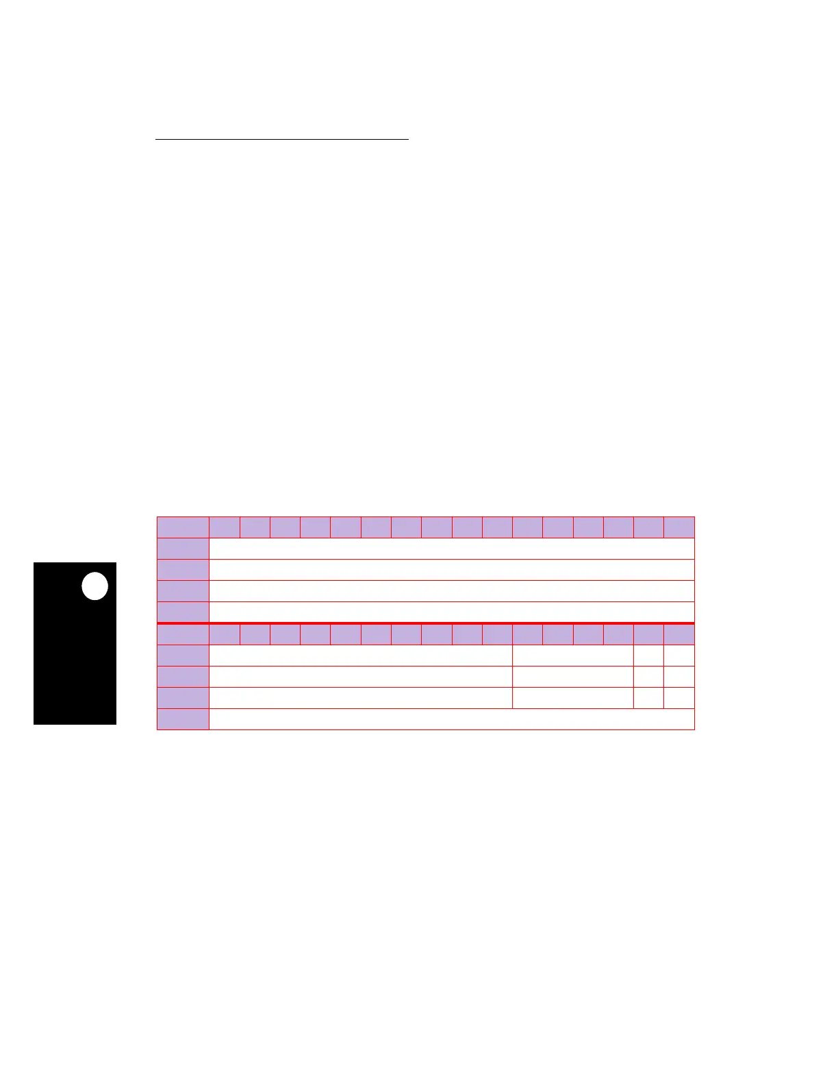
MI_RAM1
BIT 0 1 2 3 4 5 6 7 8 9 10 11 12 13 14 15
FIELD RESERVED
RESET 0
R/W R
ADDR SPR 818
BIT 16 17 18 19 20 21 22 23 24 25 26 27 28 29 30 31
FIELD RESERVED UFP PV G
RESET 0———
R/W RRRR
ADDR SPR 818
NOTE: — = Undefined.