Communication Processor Module
MOTOROLA
MPC823e REFERENCE MANUAL
16-497
PORTS
COMMUNICATION
16
PROCESSOR MODULE
16.14.11 Port D Registers
Port D has three 16-bit, memory-mapped, read/write control registers.
16.14.11.1 PORT D DATA REGISTER.
A read of the port D data (PDDAT) register returns
the data on the pins, regardless of whether the pins are an input or an output. This allows
output conflicts to be found on the pins by comparing the written data with the data on the
pins. A write to the PDDIR is latched, and if that bit in the PDDIR is configured as an output,
the value latched for that bit will be driven onto its respective pin. PDDAT can be read or
written at any time. PDDAT is not initialized and is undefined by reset.
Bits 0–2—Reserved
These bits are reserved and must be set to 0.
D3–15—Data Pins 3–15
These bits contain data can be read or written from the port D pins.
16.14.11.2 PORT D DATA DIRECTION REGISTER.
The port D data direction register
(PDDIR) is cleared at system reset.
Bits 0–2—Reserved
These bits are reserved and must be set to 0.
DR3–DR15—Data Direction Pins 3–15
0 = The corresponding pin is an input.
1 = The corresponding pin is an output.
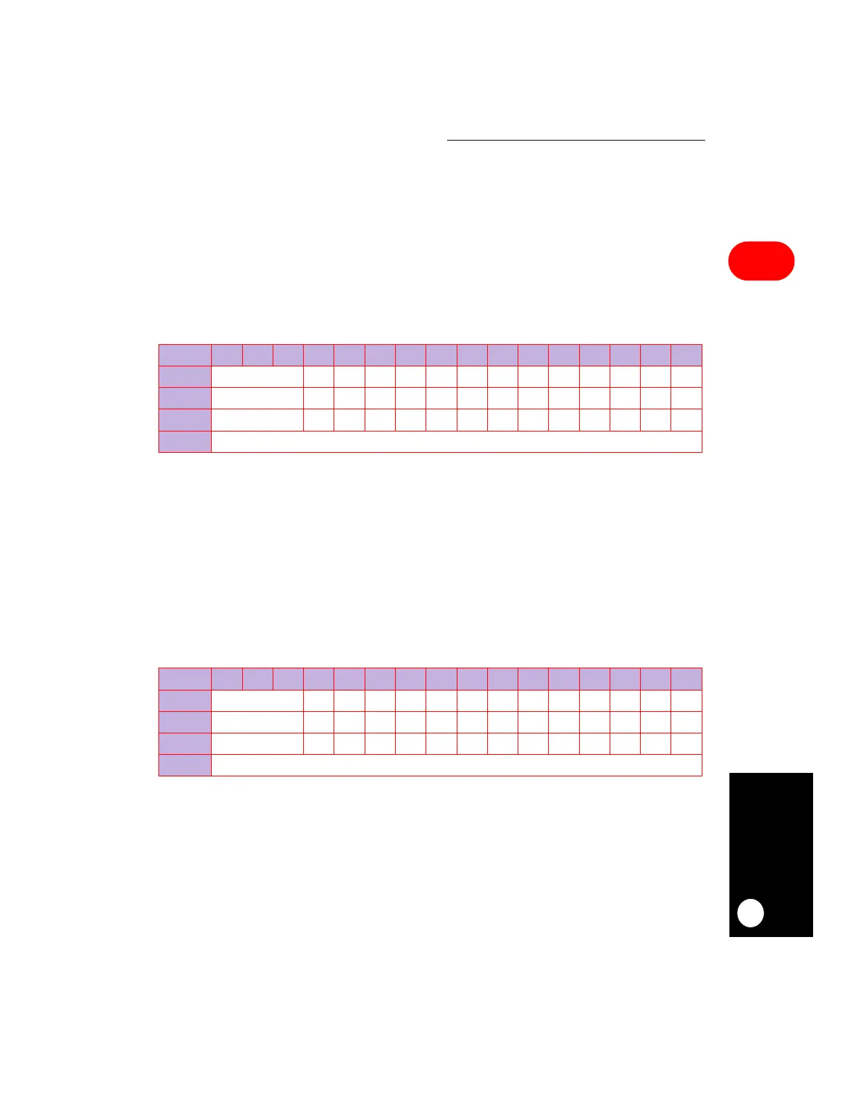
PDDAT
BIT
0 1 2 3 4 5 6 7 8 9 10 11 12 13 14 15
FIELD
RESERVED D3 D4 D5 D6 D7 D8 D9 D10 D11 D12 D13 D14 D15
RESET
— —————————————
R/W
R/W R/W R/W R/W R/W R/W R/W R/W R/W R/W R/W R/W R/W R/W
ADDR
(IMMR & 0xFFFF0000) + 0x976
NOTE: — = Undefined.
PDDIR
BIT
0 1 2 3 4 5 6 7 8 9 10 11 12 13 14 15
FIELD
RESERVED DR3 DR4 DR5 DR6 DR7 DR8 DR9 DR10 DR11 DR12 DR13 DR14 DR15
RESET
0 0000000000000
R/W
R/W R/W R/W R/W R/W R/W R/W R/W R/W R/W R/W R/W R/W R/W
ADDR
(IMMR & 0xFFFF0000) + 0x970