Communication Processor Module
MOTOROLA
MPC823e REFERENCE MANUAL
16-498
CPIC
COMMUNICATION
16
PROCESSOR MODULE
16.14.11.3 PORT D PIN ASSIGNMENT REGISTER. The port D pin assignment register
(PDPAR) is cleared at system reset.
Bits 0–2—Reserved
These bits are reserved and must be set to 0.
DD3–DD15—Dedicated Function Pins 3-15
0 = General-purpose I/O. The peripheral functions of the pin are not used.
1 = Dedicated peripheral function. The pin is used by the internal module. The on-chip
peripheral function to which it is dedicated can be determined by other bits, such
as those in the PDDIR.
16.15 THE CPM INTERRUPT CONTROLLER
The communication processor module’s interrupt controller (CPIC) is the focal point for all
interrupts associated with the communication processor module and it accepts and
prioritizes the internal and external interrupt requests from the CPM blocks. It is also
responsible for generating a vector during the core interrupt acknowledge cycle.
The CPM interrupt controller receives interrupts from such internal sources as the USB,
SCCs, SMCs, SPI, I
2
C, general-purpose timers, and port C parallel I/O pins. The CPM
interrupt controller allows you to mask each interrupt source. When multiple events within a
sub-block of the communication processor module cause the interrupt, each event is
maskable in that sub-block.
All CPM sub-block interrupt sources are prioritized and bits are set in the CPM interrupt
pending register (CIPR) where all interrupt sources are assigned one programmable priority
level (0–7) before the request for an interrupt is sent to the U-Bus. An overview of the
MPC823e interrupt structure is illustrated in Figure 16-135. The lower half of the figure
illustrates the CPM interrupt controller.
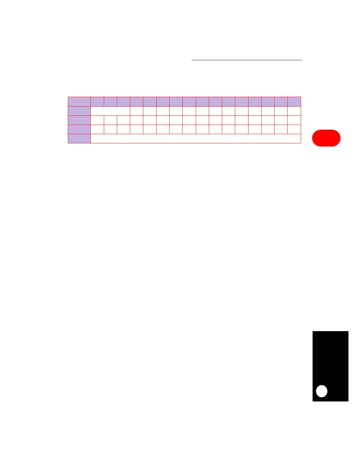
PDPAR
BIT 0 1 2 3 4 5 6 7 8 9 10 11 12 13 14 15
FIELD RESERVED DD3 DD4 DD5 DD6 DD7 DD8 DD9 DD10 DD11 DD12 DD13 DD14 DD15
RESET 0000000000000000
R/W R/W R/W R/W R/W R/W R/W R/W R/W R/W R/W R/W R/W R/W R/W R/W R/W
ADDR (IMMR & 0xFFFF0000) + 0x972