Memory Management Unit
MOTOROLA MPC823e REFERENCE MANUAL 11-41
MEMORY MANAGEMENT
11
UNIT
11.6.2.3 MMU DATA RAM ENTRY READ REGISTER 1. The MMU data RAM entry read
register 1 (MD_RAM1) contains the protection mode information of the entry indexed by the
DTLB_INDX field of the MD_CTR. This register is only updated when you write a value to it.
Bits 0–16—Reserved
These bits are reserved and must be set to 0.
C—Change Bit for Data Entry TLB
0 = Unchanged region. Write access to this page results in the implementation-specific
instruction MMU interrupt invocation. Software must take an appropriate action
before setting this bit to 1.
1 = Changed region. Write access is allowed to this page.
EVF—Entry Valid Flag
0 = Entry is invalid.
1 = Entry is valid.
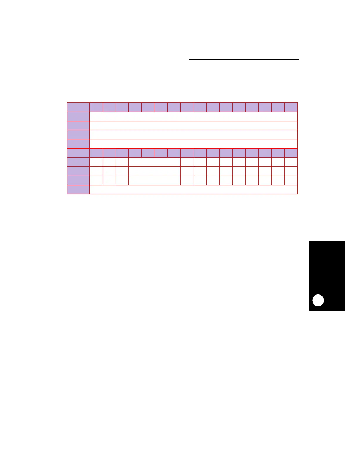
MD_RAM1
BIT 0 1 2 3 4 5 6 7 8 9 10 11 12 13 14 15
FIELD
RESERVED
RESET
0
R/W
R
ADDR
SPR 826
BIT 16 17 18 19 20 21 22 23 24 25 26 27 28 29 30 31
FIELD
RES C EVF SA SAT URP0 UWP0 URP1 UWP1 URP2 UWP2 URP3 UWP3
RESET
0 —— — —————————
R/W
RRR R RRRRRRRRR
ADDR
SPR 826
NOTE: — = Undefined.