IEEE 1149.1 Test Access Port
MOTOROLA MPC823e REFERENCE MANUAL 21-19
IEEE 1149.1 TEST
21
ACCESS PORT
21.3 THE INSTRUCTION REGISTER
The MPC823e JTAG implementation includes the public instructions—extest, sample/
preload, bypass, and clamp. One additional public instruction—hi-z—is capable of
disabling all device output drivers. The MPC823e includes a 4-bit instruction register that
consists of a shift register with four parallel outputs. Data is transferred from the shift register
to the parallel outputs during the update-IR controller state. The four bits are used to decode
the five unique instructions listed in Table 21-2.
The parallel output of the instruction register is reset to all ones in the test-logic-reset
controller state. Notice that this preset state is equivalent to the bypass instruction. During
the capture-IR controller state, the parallel inputs to the instruction shift register are loaded
with the clamp command code.
21.3.1 The External Test Instruction
The external test (extest) instruction selects the 397-bit boundary scan register and asserts
an internal reset for the MPC823e system logic to force a known beginning internal state
while performing external boundary scan operations. By using the TAP controller, the
register is capable of scanning user-defined values into the output buffers, capturing values
presented to the input pins, and controlling the output drive of three-stateable output or
bidirectional pins. For more details on the function and use of extest, refer to the IEEE
1149.1 standard.
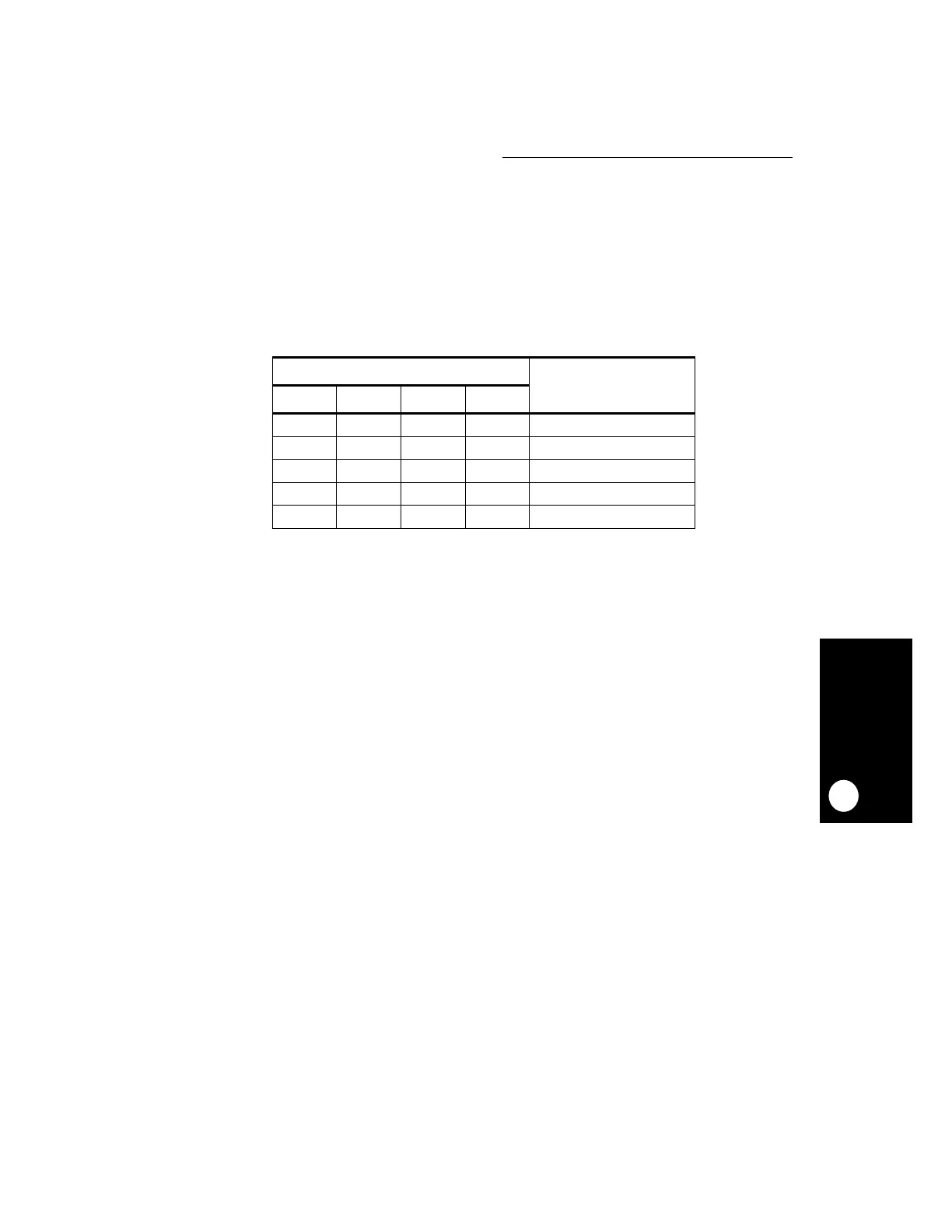
Table 21-2. Instruction Decoding
CODE INSTRUCTION
B3 B2 B1 B0
0000 EXTEST
0001SAMPLE/PRELOAD
0X1X BYPASS
0100 HI-Z
101CLAMP and BYPASS
NOTE:
B0 (LSB) is shifted first.
 Loading...

