Memory Controller
MOTOROLA
MPC823e REFERENCE MANUAL
15-5
MEMORY CONTROLLER
15
Some features are common to all eight memory banks. The full 32-bit decode is available
internally, even if all 32 address bits are not visible outside the MPC823e. For external
master transactions, the memory controller extends the 26-bit external address line to 32
bits and the six most-significant bits are zero. The variable block size of each memory bank
can be between 32K and 64M for a total memory capacity of 512M. Parity can be generated
and checked for any memory bank and each memory bank can be selected for read-only or
read/write operation. For system protection purposes, you can use certain address type
codes to cause the memory controller to restrict access to a memory bank. For additional
flexibility, address type comparisons provide you with a mask option.
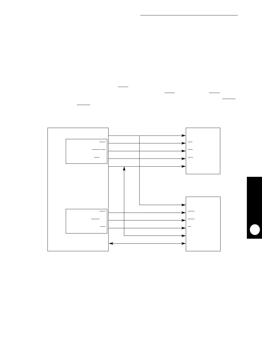
The memory controller functionality helps you design MPC823e-based systems with little or
no glue logic required. In Figure 15-3, CS0
is used as the 16-bit boot EPROM with the MS
field of the base register 0 configured to select the GPCM. CS1
is used as the RAS signal
for 32-bit DRAM with the MS field of base register 1 configured to select UPMA. The BS_A
signals are used as CASx
signals on the DRAM.
MPC823e
Figure 15-3. Simple System Configuration
CE
OE
W
EPROM
ADDRESS
WE
DATA
DRAM
ADDRESS
RAS
CAS[0:3]
DATA
PARITY
CS1
WE[0:1]
RD/WR
GPL1/OE
DP[0:3]
ADDRESS
DATA
CS0
BS_A[0:3]
GPCM
UPMA