Memory Controller
15-34 MPC823e REFERENCE MANUAL MOTOROLA
MEMORY CONTROLLER
15
15.4.1.1 PROGRAMMABLE WAIT STATE CONFIGURATION. The general-purpose
chip-select machine supports internal TA
signal generation. It allows “fast” accesses to
external memory through an internal bus master or it allows a maximum 17-clock access.
This can be done by programming the SCY field in the option register. The internal TA
generation mode is enabled if the SETA field in the option register is cleared. If the TA
pin
is externally asserted at least two clock cycles before the wait state counter has expired, the
current memory cycle is terminated. When the TRLX bit is set, the number of wait states
inserted by the memory controller is defined by 2 x SCY or a maximum of 30 wait states.
15.4.1.2 EXTENDED HOLD TIME ON READ ACCESSES. Slow memory devices that
require a long delay on data read accesses must set the EHTR field in the corresponding
option register. Any GPCM access to the external bus following a read access to the slower
memory bank is delayed by one clock cycle, unless it is a read access to the same bank.
Refer to Figure 15-13 through Figure 15-16 for details.
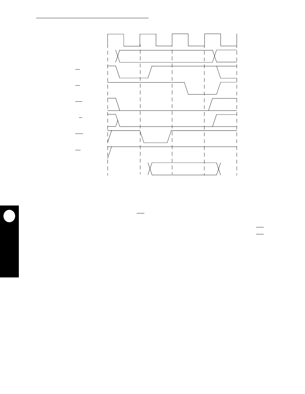
Figure 15-12. MPC823e GPCM–Relaxed Timing–Write Access
(ACS = 00, SCY = 0, CSNT = 1, and TRLX = 1)
CLOCK
ADDRESS
TS
TA
CSx
R/W
WEx
DATA
OE
 Loading...

