Memory Controller
15-60 MPC823e REFERENCE MANUAL MOTOROLA
MEMORY CONTROLLER
15
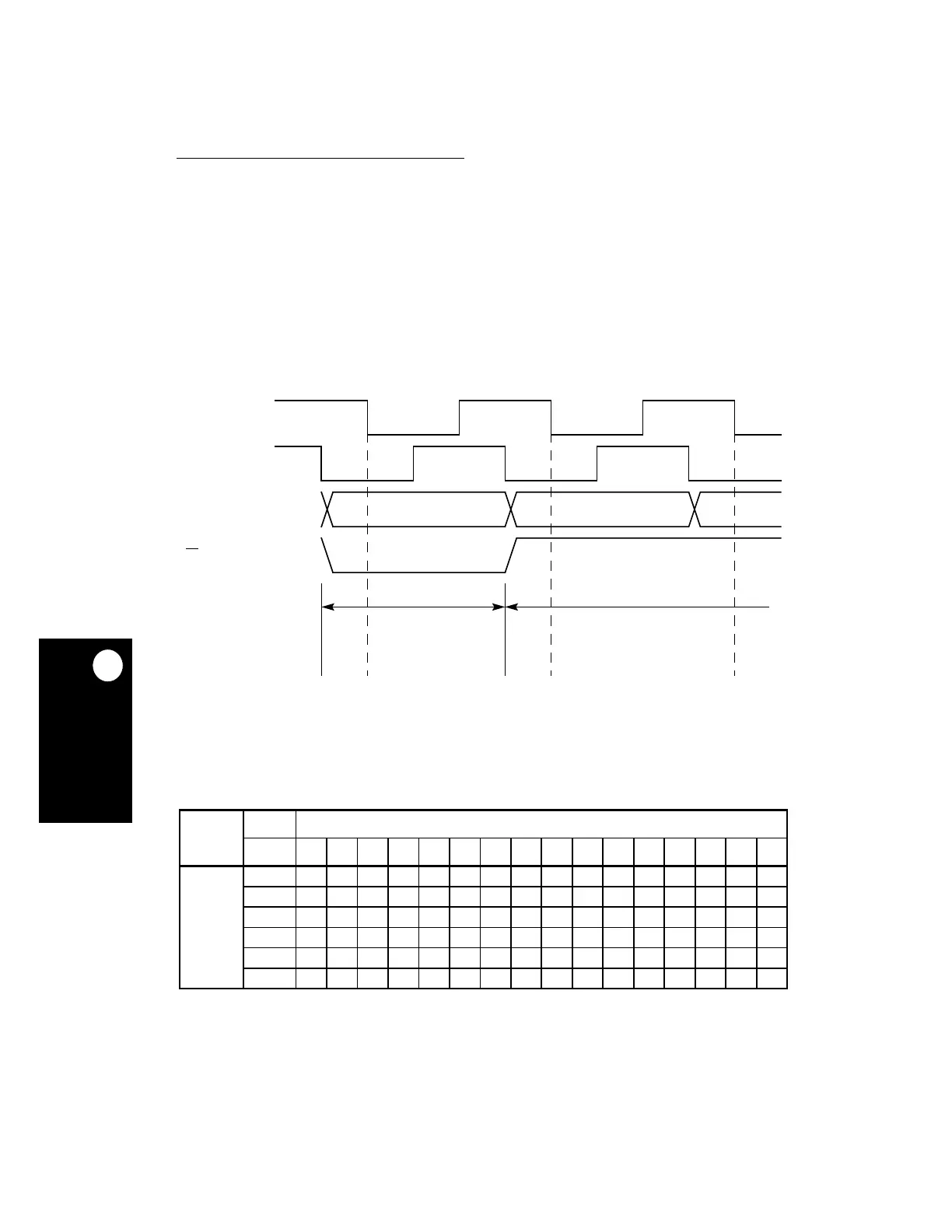
15.5.4.2.7 Address Multiplexing. You can control the address signals that go to the
external bus. The AMA and AMB fields of the MxMR control how the address signals are
multiplexed. The SAM bit in the option register determines the address multiplexing for the
first clock cycle. The AMX field in the RAM word determines the multiplexing for subsequent
clock cycles. The lower address pins can be multiplexed between the internal upper or lower
address signals. The SAM bit outputs the upper address signals and the AMX field outputs
the lower address signals. Using the AMX field, you can output the contents of the memory
address register (MAR) on the address pins. See Table 15-6 for general configuration.
Table 15-7 shows how the AMA and AMB fields can be defined to interface with a wide
range of DRAM modules. Figure 15-31 illustrates address multiplex timing.
Figure 15-31. Address Multiplex Timing
Table 15-7. Address Multiplexing
PINS
AMA/AMB A16 A17 A18 A19 A20 A21 A22 A23 A24 A25 A26 A27 A28 A29 A30 A31
SIGNALS
000 RES RES A10 A11 A12 A13 A14 A15 A16 A17 A18 A19 A20 A21 A22 A23
001 RES A8 A9 A10 A11 A12 A13 A14 A15 A16 A17 A18 A19 A20 A21 A22
010 A6 A7 A8 A9 A10 A11 A12 A13 A14 A15 A16 A17 A18 A19 A20 A21
011 RES A6 A7 A8 A9 A10 A11 A12 A13 A14 A15 A16 A17 A18 A19 A20
100 A4 A5 A6 A7 A8 A9 A10 A11 A12 A13 A14 A15 A16 A17 A18 A19
101 RES A4 A5 A6 A7 A8 A9 A10 A11 A12 A13 A14 A15 A16 A17 A18
CLKOUT/GCLK2
GCLK1
TS
RAM WORD 1 RAM WORD 2
A[0:31]
ADDRESS CONTROLLED
BY SAM
ADDRESS CONTROLLED
BY AMX
UPPER ADDRESS LOWER ADDRESS
 Loading...

