Memory Controller
MOTOROLA
MPC823e REFERENCE MANUAL
15-89
MEMORY CONTROLLER
15
MEMORY CONTROLLER
15
4. Define the UPMB (or UPMA) parameters that control the memory system in the
following sequence. For additional details, see Table 15-11.
— Program the RAM array using the memory command register (MCR) and
memory data register (MDR). The RAM word must be written into the MDR
before you issue the
WRITE
command to the MCR. Repeat this step for all RAM
word entries.
— Initialize the option and base registers of the specific bank according to the
address mapping of the DRAM device you have chosen.
— Use the MS field of the option register to select the machine you have chosen
to control the cycles. Notice that the SAM bit in the option register determines
address multiplexing for the first clock cycle and subsequent cycles are
controlled by the UPM RAM words. Also notice that the AMX field in the UPM
RAM word controls the address multiplexing for the next clock cycle rather than
the current cycle.
— Program the MBMR to select the number of columns and refresh timer
parameters.
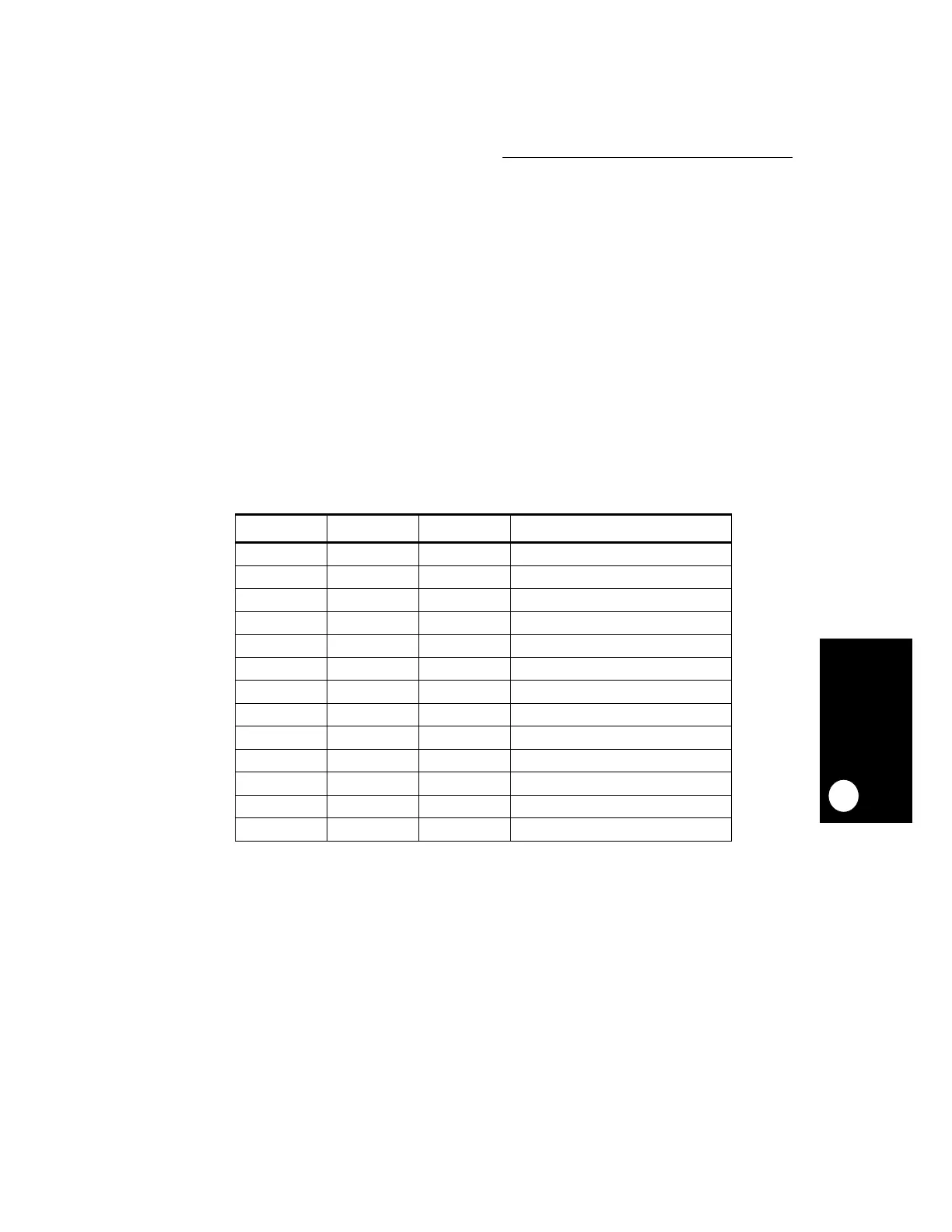
Table 15-11. UPMB Register Settings
FIELD REGISTER VALUE COMMENTS
MS BR2 10 Selects UPMB
PS BR2 00 Selects 32-Bit Bus Width
WP BR2 0 Allows Read and Write Accesses
PTP MPTPR 00000010 Prescaler Divided by 32
PTB MBMR 00001100 15.6
µ
s at a 25MHz Clock
PTBE MBMR 1 Enables Periodic Timer B
AMB MBMR 001 Selects Nine Column Address Pins
DSB MBMR 01 Selects Two Disable Timer Clock Cycles
GPLB4DIS MBMR 0 Disables the UPWAITB Signal
RLFB MBMR 0011 Selects Three Loop Iterations for Read
WLFB MBMR 0011 Selects Three Loop Iterations for Write
SAM OR2 1 Selects Column Address on First Cycle
BI OR2 0 Supports Burst Accesses
 Loading...

