Communication Processor Module
MOTOROLA
MPC823e REFERENCE MANUAL
16-77
COMMUNICATION
16
PROCESSOR MODULE
TIMERS
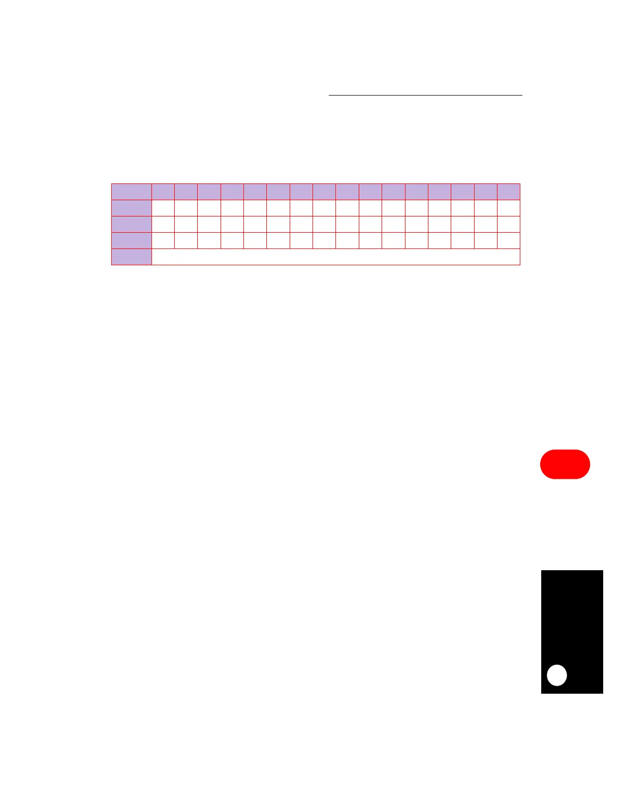
16.4.2.2 TIMER GLOBAL CONFIGURATION REGISTER.
The 16-bit, memory-mapped,
read/write timer global configuration register (TGCR) contains configuration parameters that
are used by both timers. It allows simultaneous starting and stopping of any number of
timers as long as one bus cycle is used to access TGCR.
CAS4—Cascade Timers
0 = Normal operation.
1 = Timers 3 and 4 are cascaded to form a 32-bit timer.
FRZ4–FRZ1—Freeze
0 = The corresponding timer ignores the FRZ pin.
1 = Stops the corresponding timer if the FRZ pin is asserted by the core during
breakpoint.
STP4–STP1 —Stop Timer
0 = Normal operation.
1 = Reduce the timer’s power consumption. This bit stops all clocks to the timer, except
the clock from the U-Bus interface, which allows you to read and write the timer
registers. The clocks to the timer remain inactive until you clear this bit or a
hardware reset occurs.
RST4–RST1—Reset Timer
0 = Reset the corresponding timer. A software reset is identical to an external reset.
1 = Enable the corresponding timer if the STPx bit is cleared.
Bit 4—Reserved
This bit is reserved and must be set to 0.
CAS2—Cascade Timers
0 = Normal operation.
1 = Timers 1 and 2 are cascaded to form a 32-bit timer.
TGCR
BIT
0 1 2 3 4 5 6 7 8 9 10 11 12 13 14 15
FIELD
CAS4 FRZ4 STP4 RST4 RES FRZ3 STP3 RST3 CAS2 FRZ2 STP2 RST2 GM1 FRZ1 STP1 RST1
RESET
0000000000000000
R/W
R/W R/W R/W R/W R/W R/W R/W R/W R/W R/W R/W R/W R/W R/W R/W R/W
ADDR
(IMMR & 0xFFFF0000) + 0x980

 Loading...