Communication Processor Module
16-136 MPC823e REFERENCE MANUAL MOTOROLA
SERIAL
I/F
COMMUNICATION
16
PROCESSOR MODULE
16.7.5.3 SERIAL INTERFACE CLOCK ROUTE REGISTER. The 32-bit, read/write,
memory-mapped serial interface clock route (SICR) register is used to define the universal
serial bus and serial communication controller clock sources that can be one of the four
baud rate generators or an input from a bank of clock pins.
Bits 0–7—Reserved
These bits are reserved and must be set to 0.
GR3—Grant Support of SCC3
0 = SCC3 transmitter does not support the grant mechanism. The grant is always
asserted internally.
1 = SCC3 transmitter supports the grant mechanism as determined by the GMx bit
of the SIMODE register.
SC3—SCC3 Connection
0 = SCC3 is not connected to the multiplexed serial interface but is either connected
directly to the NMSI3 pins or is not used. You can choose either the
general-purpose I/O port pins or dedicated SCC3 pins in the parallel I/O port
registers. See Section 16.14 The Parallel I/O Ports for more information.
1 = SCC3 is connected to the multiplexed serial interface. The NMSI3 receive pins are
available for other purposes.
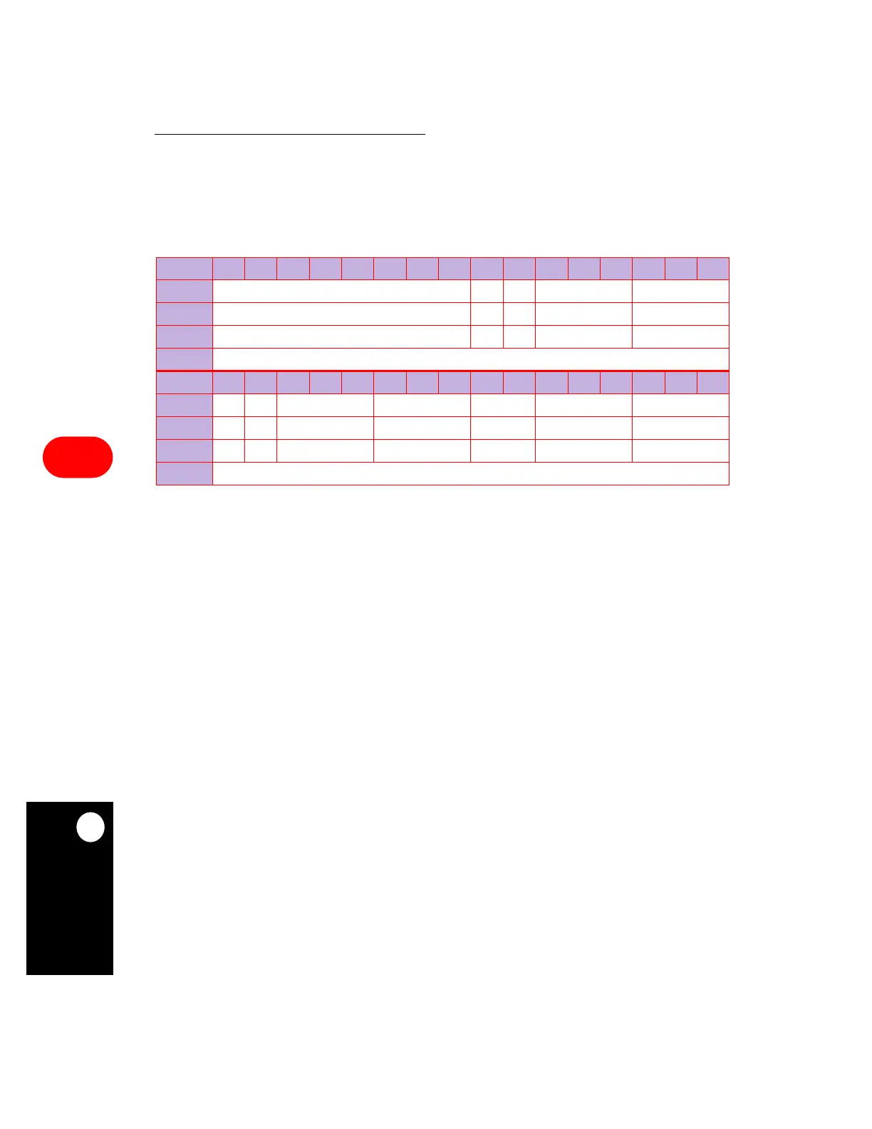
SICR
BIT 0 1 2 3 4 5 6 7 8 9 10 11 12 13 14 15
FIELD RESERVED GR3 SC3 R3CS T3CS
RESET 00000
R/W R/W R/W R/W R/W R/W
ADDR (IMMR & 0xFFFF0000) + 0xAEC
BIT 16 17 18 19 20 21 22 23 24 25 26 27 28 29 30 31
FIELD GR2 SC2 R2CS T2CS RES R1CS RESERVED
RESET 000 000 0
R/W R/W R/W R/W R/W R/W R/W R/W
ADDR (IMMR & 0xFFFF0000) + 0xAEE
 Loading...

