Communication Processor Module
16-184 MPC823e REFERENCE MANUAL MOTOROLA
SCCs
COMMUNICATION
16
PROCESSOR MODULE
• RFCR and TFCR—There are two function code registers for the SCCx channel—one
for receive data buffers and one for transmit data buffers. The function code entry
contains the value that you want to appear on the AT pins when the associated SDMA
channel accesses memory. It also controls the byte-ordering convention for transfers.
Bits 0–2—Reserved
These bits are reserved and must be set to 0.
BO—Byte Ordering
You must set these bits to select the required byte ordering of the data buffer. If this field
is modified on-the-fly, it takes effect at the beginning of the next frame or the next buffer
descriptor.
00 = The DEC/Intel convention is used for byte ordering (swapped operation) and
is also called little-endian byte ordering. The transmission order of bytes within
a buffer word is reversed in comparison to the Motorola mode. This mode is
supported only for 32-bit port size memory.
01 = PowerPC little-endian byte ordering. As data is transmitted onto the serial line
from the data buffer, the least-significant byte of the buffer double-word
contains data to be transmitted earlier than the most-significant byte of the
same buffer double-word.
1X = Motorola byte ordering (normal operation) is also called big-endian byte
ordering. As data is transmitted onto the serial line from the data buffer, the
most-significant byte of the buffer word contains data to be transmitted earlier
than the least-significant byte of the same buffer word.
AT—Address Type
These bits contain the function code value used during the SDMA channel memory
access. AT0 is driven with a 1 to identify this SDMA channel access as a DMA type.
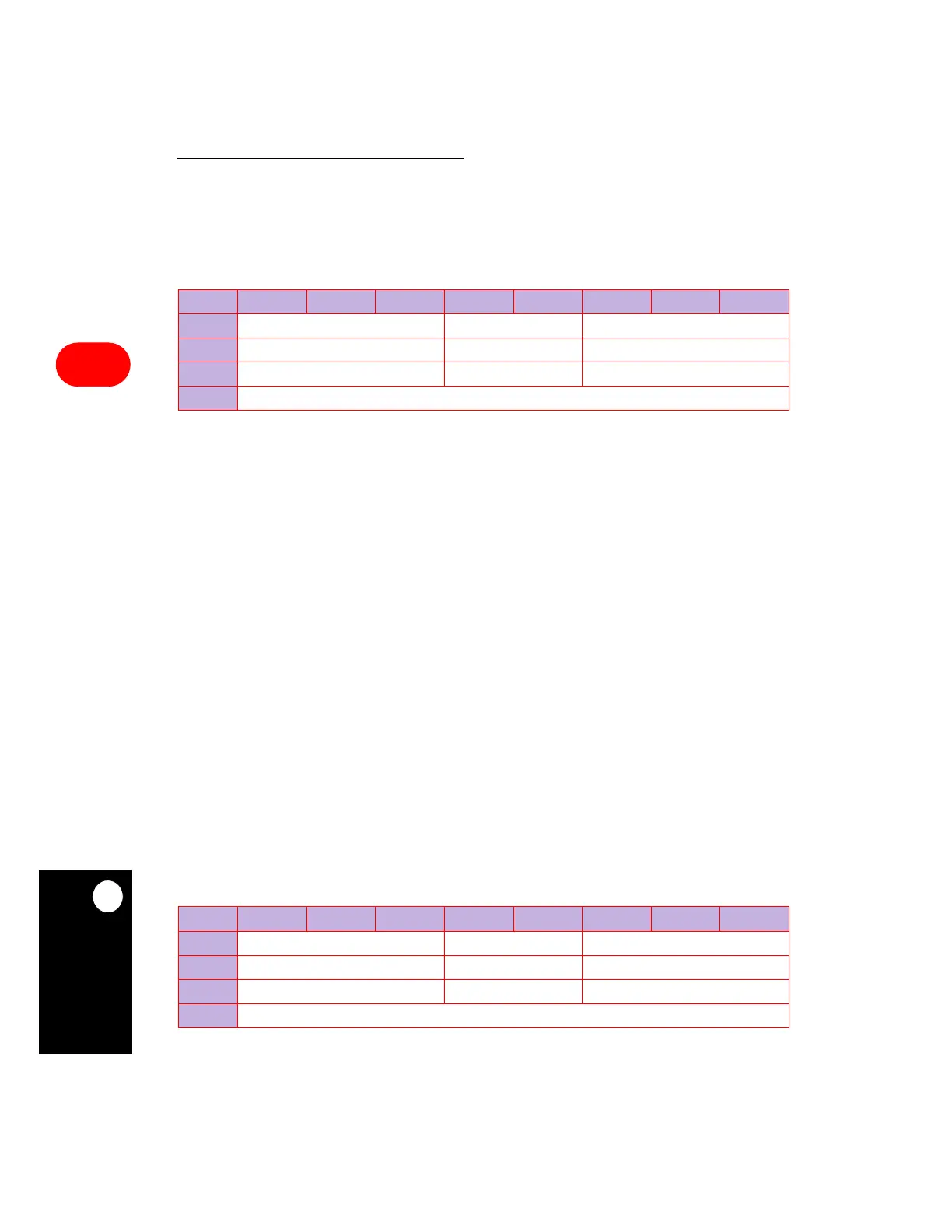
RFCR
BIT 0 1 2 3 4 5 6 7
FIELD RESERVED BO AT
RESET 000
R/W R/W R/W R/W
ADDR SCCX BASE + 0x00
TFCR
BIT 0 1 2 3 4 5 6 7
FIELD RESERVED BO AT1–AT3
RESET 000
R/W R/W R/W R/W
ADDR SCCX BASE + 0x02