Communication Processor Module
MOTOROLA
MPC823e REFERENCE MANUAL
16-217
COMMUNICATION
16
SCCs
16.9.15.15 SCCx UART MODE REGISTER.
When a serial communication controller is in
UART mode, the 16-bit, memory-mapped, read/write protocol-specific mode register is
referred to as the SCCx UART mode register (PSMR–SCC UART). Since each protocol has
specific requirements, the PSMR bits are different for each implementation. Many of the bits
can be modified on-the-fly while the receiver and transmitter are enabled.
FLC—Flow Control
0 = Normal operation. The GSMR_x and port C registers determine the mode of the
CTSx
pin.
1 = Asynchronous flow control. When the CTSx
pin is negated, the transmitter stops at
the end of the current character. If CTSx
is negated past the middle of the current
character, the next full character can be sent and transmission is stopped. When
CTSx
is asserted once more, transmission continues where it left off and no CTSx
lost error is reported. No characters except idles are transmitted while CTSx
is
negated.
SL—Stop Length
This bit selects the number of stop bits transmitted by the SCCx UART controller. It can be
modified on-the-fly. The receiver is always enabled for one stop bit unless the SCCx UART
controller is in synchronous mode and the RZS bit is set. Fractional stop bits are configured
in the general DSR, which is described in
Section 16.9.4 Data Synchronization Register
.
0 = One stop bit.
1 = Two stop bits.
CL—Character Length
This field determines the number of data bits in the character, not including the optional
parity or multidrop address bits. When you use a character that is less than 8 bits, the
most-signifiant bits in memory are written as zeros and they are labeled “don’t care” when
they are transmitted. This field can be modified on-the-fly.
00 = 5 data bits.
01 = 6 data bits.
10 = 7 data bits.
11 = 8 data bits.
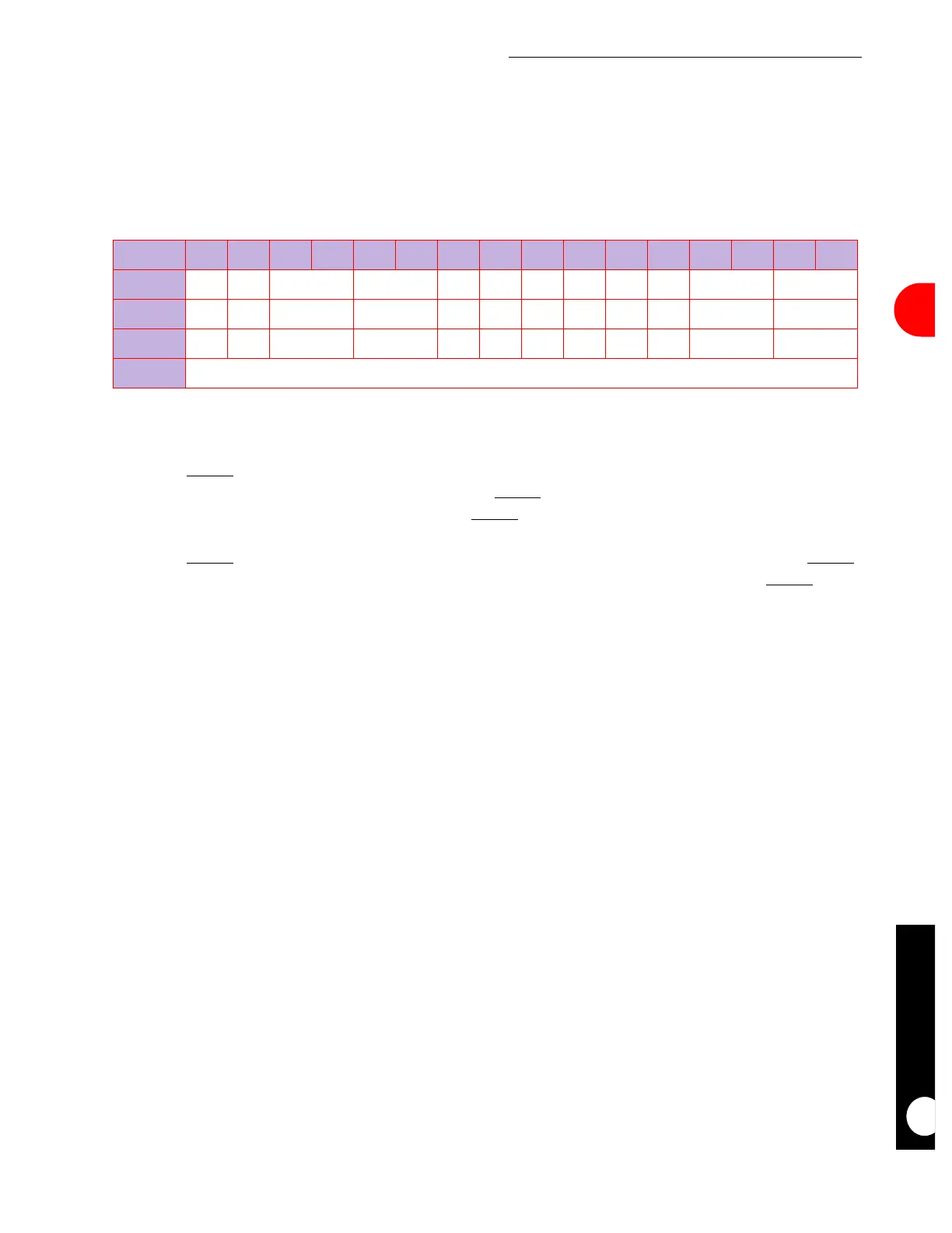
PSMR–SCC UART
BIT 0 1 2 3 4 5 6 7 8 9 10 11 12 13 14 15
FIELD
FLC SL CL UM FRZ RZS SYN DRT RES PEN RPM TPM
RESET
00 0 0 000000 0 0
R/W
R/W R/W R/W R/W R/W R/W R/W R/W R/W R/W R/W R/W
ADDR
(IMMR & 0xFFFF0000) + 0xA28 (SCC2 AND A48 (SCC3)