External Signals
MOTOROLA MPC823e REFERENCE MANUAL 2-9
EXTERNAL SIGNALS
2
PA[5]
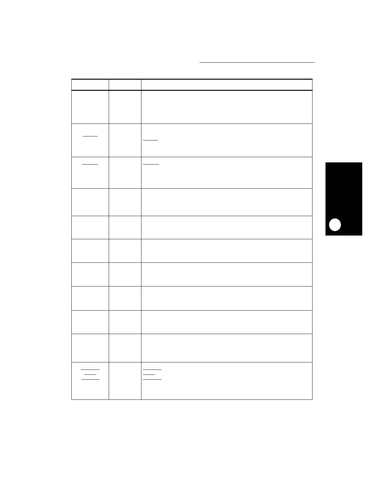
CLK3
TIN2
L1TCLKA
BRGO2
T6 General-Purpose I/O Port A Bit 5—Bit 5 of the general-purpose I/O port A.
CLK3—This input signal is one of the four clock pins that can be used to clock the
serial communication controllers, serial management controllers, and USB.
TIN2—The timer 2 external clock input pin.
L1TCLKA—The transmit clock for the serial interface time-division multiplex port A.
BRGO2—The output clock of BRG2.
PA[4]
CLK4
TOUT2
TIN4
L1TCLKB
R6 General-Purpose I/O Port A Bit 4—Bit 4 of the general-purpose I/O port A.
CLK4—This input signal is one of the four clock pins that can be used to clock the
serial communication controllers, serial management controllers, and USB.
TOUT2
—The timer 2 output pin.
TIN4—The timer 4 external clock pin.
L1TCLKB—The transmit clock for the serial interface time-division multiplex port A.
PB[31]
SPISEL
LCD_A
N14 General-Purpose I/O Port B Bit 31—Bit 31 of the general-purpose I/O port B.
SPISEL
—The serial peripheral interface slave select input pin.
LCD_A—This is one of the LCD controller’s three extension data bits, which are
used to drive an active LCD panel. When using a 12-bit bus instead of a 9-bit bus,
the LCD_A signal is the least-significant bit of the red 4-bit code. The red portion of
the bus consists of LD[0:2] and LCD_A.
PB[30]
SPICLK
TXD3
P15 General-Purpose I/O Port B Bit 30—Bit 30 of the general-purpose I/O port B.
SPICLK—The serial peripheral interface output clock when it is configured as a
master or serial peripheral interface input clock when it is configured as a slave.
TXD3—The transmit data output signal for serial communication controller 3. TXD3
has open-drain capability.
PB[29]
SPIMOSI
RXD3
P14 General-Purpose I/O Port B Bit 29—Bit 29 of the general-purpose I/O port B.
SPIMOSI—The serial peripheral interface output data when it is configured as a
master or serial peripheral interface input data when it is configured as a slave.
RXD3—The receive data input signal for serial communication controller 3.
PB[28]
SPIMISO
BRGO3
T15 General-Purpose I/O Port B Bit 28—Bit 28 of the general-purpose I/O port B.
SPIMISO—The serial peripheral interface input data when it is configured as a
master or serial peripheral interface output data when it is configured as a slave.
BRGO3—The output clock of BRG3.
PB[27]
I2CSDA
BRGO1
T14 General-Purpose I/O Port B Bit 27—Bit 27 of the general-purpose I/O port B.
I2CSDA—The I
2
C serial data pin. This pin is bidirectional and should be configured
as an open-drain output.
BRGO1—The output clock of BRG1.
PB[26]
I2CSCL
BRGO2
P12 General-Purpose I/O Port B Bit 26—Bit 26 of the general-purpose I/O port B.
I2CSCL—The I
2
C serial clock pin. This pin is bidirectional and should be configured
as an open-drain output.
BRGO2—The output clock of BRG2.
PB[25]
SMTXD1
TXD3
N11 General-Purpose I/O Port B Bit 25—Bit 25 of the general-purpose I/O port B.
SMTXD1—The serial management controller 1 transmit data output pin.
TXD3—The transmit data output signal for serial communication controller 3. TXD3
has open-drain capability.
PB[24]
SMRXD1
RXD3
L1RXDB
T11 General-Purpose I/O Port B Bit 24—Bit 24 of the general-purpose I/O port B.
SMRXD1—The serial management controller 1 receive data input pin.
RXD3—The receive data input signal for serial communication controller 3.
L1RXDB—The receive data input signal for the serial interface time-division
multiplex port B.
PB[23]
SMSYN1
CTS3
SDACK1
L1RSYNCB
T10 General-Purpose I/O Port B Bit 23—Bit 23 of the general-purpose I/O port B.
SMSYN1
—The serial management controller 1 external sync input pin.
CTS3
—The Clear to Send Modem line for serial communication controller 3.
SDACK1
—The SDMA acknowledge 1 output pin that is used as a peripheral
interface signal for IDMA emulation.
L1RSYNCB—The transmit sync input for the serial interface time-division multiplex
port B.
Table 2-1. Signal Descriptions (Continued)
SIGNAL PIN NUMBER DESCRIPTION