Communication Processor Module
MOTOROLA MPC823e REFERENCE MANUAL 16-443
SPI
COMMUNICATION
16
PROCESSOR MODULE
16.12.4 Programming the Serial Peripheral Interface
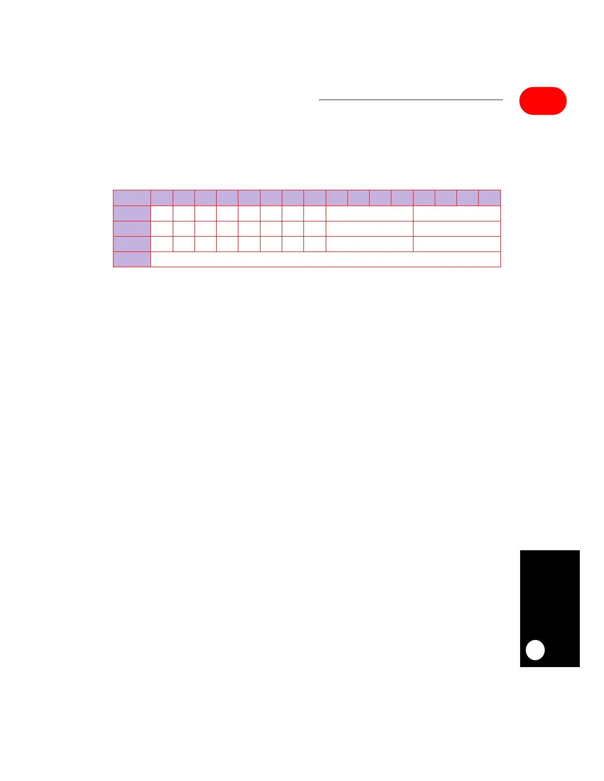
16.12.4.1 SPI MODE REGISTER. The read/write SPI mode (SPMODE) register controls
both the serial peripheral interface operation mode and clock source. Table 16-2 contains
more information on commands that can be used with this register.
Bit 0—Reserved
This bit is reserved and must be set to 0.
LOOP—Loop Mode
When set, this bit selects the local loopback operation. The transmitter output is internally
connected to the receiver input. The receiver and transmitter operate normally, except that
the externally received data is ignored.
0 = Normal operation.
1 = The serial peripheral interface is in loopback mode.
CI—Clock Invert
This bit inverts the SPI clock polarity. See Figure 16-124 and Figure 16-125 for details.
0 = The inactive state of SPICLK is low.
1 = The inactive state of SPICLK is high.
CP—Clock Phase
This bit selects one of two fundamentally different transfer formats. See Figure 16-124 and
Figure 16-125 for details.
0 = SPICLK starts toggling at the middle of the data transfer.
1 = SPICLK starts toggling at the beginning of the data transfer.
DIV16—Divide by 16
This bit selects the clock source for the SPI baud rate generator when configured as an SPI
master. In slave mode, the clock source is the SPICLK pin.
0 = Use the BRGCLK as the input to the SPI baud rate generator.
1 = Use the BRGCLK/16 as the input to the SPI baud rate generator.
SPMODE
BIT 0 1 2 3 4 5 6 7 8 9 10 11 12 13 14 15
FIELD
RES LOOP CI CP DIV16 REV M/S EN LEN PM
RESET
00000000 0 0
R/W
R/W R/W R/W R/W R/W R/W R/W R/W R/W R/W
ADDR
(IMMR & 0xFFFF0000) + 0xAA0
 Loading...