Communication Processor Module
MOTOROLA
MPC823e REFERENCE MANUAL
16-489
PORTS
COMMUNICATION
16
PROCESSOR MODULE
16.14.7 Port B Configuration Example
You can configure the PB31 pin as a general-purpose I/O or open-drain pin. It can also be
the LCD_A pin for the LCD controller or the SPI select input SPISEL pin. If PB31 is not
configured to connect to the LCD_A or SPISEL
signal, then the serial peripheral interface
receives V
DD
on that signal.
16.14.8 Port C Pin Functionality
Port C consists of 12 general-purpose I/O pins that have interrupt capability. Refer to
Table 16-43 for a description of all port C pin options.
All PCDIR and PCPAR bits are cleared by a total system reset, which configures all port pins
as general-purpose input pins. Notice that the global CPM interrupt mask register is also
cleared when a total system reset occurs, so if any port C pin is left floating it does not cause
a false interrupt.
If a port C pin is selected as a general-purpose I/O pin, it can be accessed through the
PCDAT register where written data is stored in an output latch. If a port C pin is configured
as an output, the output latch data is gated onto the port pin. When the PCDAT register is
read, the port pin itself is read. If a port C pin is configured as an input, data written to PCDAT
register is still stored in the output latch, but is prevented from reaching the port pin. In this
case, when PCDAT register is read, the state of the port pin is read.
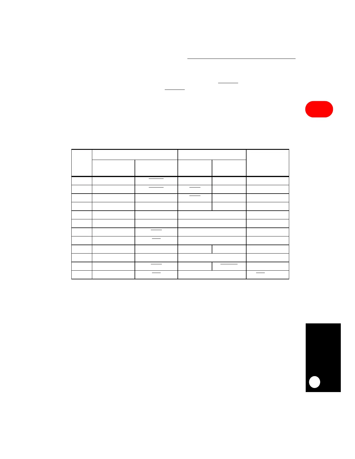
Table 16-43. Port C Pin Assignment
SIGNAL PCPAR = 0 PCPAR = 1 INPUT TO ON-CHIP
PERIPHERALS
PCDIR = 1 OR
PCSO = 0
PCDIR = 0 AND
PCSO = 1
PCDIR = 0 PCDIR = 1
PC15 Port C15 DREQ1
L1TXDB L1ST5 EXT0 = VDD
PC14 Port C14 DREQ2 RTS2 L1ST6 EXT1 = VDD
PC13 Port C13 — RTS3 L1ST7 —
PC12 Port C12 — L1RQA L1ST8 —
PC11 Port C11 USBRXP — GND
PC10 Port C10 USBRXN TGATE1 GND
PC9 Port C9 CTS2 — GND
PC8 Port C8 CD2 TGATE1 GND
PC7 Port C7 — — USBTXP —
PC6 Port C6 — USBTXN —
PC5 Port C5 CTS3 L1TSYNCA SDACK1 —
PC4 Port C4 CD3 L1RSYNCA CD3 = GND