Communication Processor Module
MOTOROLA
MPC823e REFERENCE MANUAL
16-493
PORTS
COMMUNICATION
16
PROCESSOR MODULE
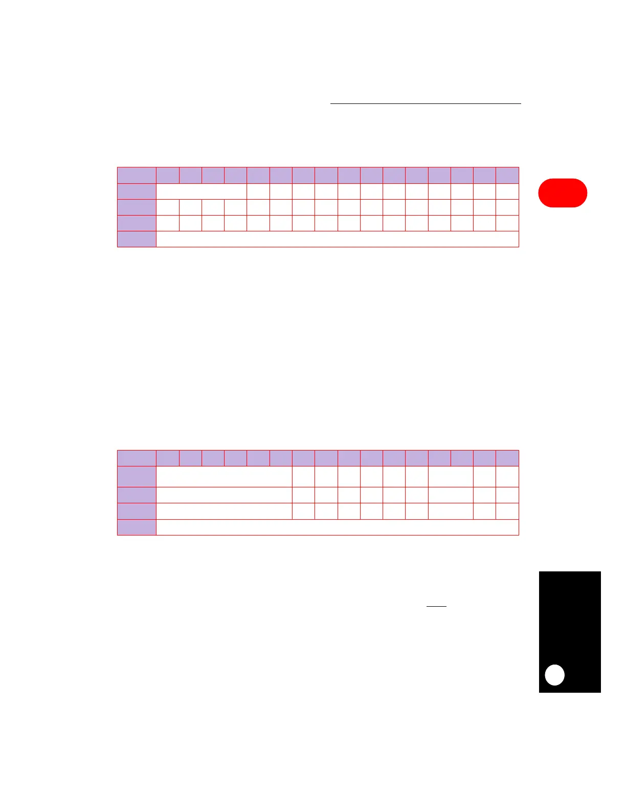
16.14.9.3 PORT C PIN ASSIGNMENT REGISTER.
The port C pin assignment register
(PCPAR) is a 16-bit register that is cleared by system reset.
Bits 0–3—Reserved
These bits are reserved and must be set to 0.
DD4–DD15—Dedicated Function Pins 4-15
0 = General-purpose I/O. The peripheral functions of the pin are not used.
1 = Dedicated peripheral function. The pin is used by the internal module. The on-chip
peripheral function to which it is dedicated can be determined by other bits such as
those in the PBDIR.
16.14.9.4 PORT C SPECIAL OPTIONS REGISTER.
The port C special options (PCSO)
register indicates whether certain port C pins can connect to on-chip peripherals and
generate an interrupt at the same time. Each bit defined in the PCSO corresponds to a port
C line (PC8–PC11 and PC14–PC15). The PCSO is cleared by reset.
Bits 0–5 and 12–13—Reserved
These bits are reserved and must be set to 0.
CDx—Carrier Detect 2 and 3
0 = PCx is a general-purpose interrupt I/O pin. The SCCx internal CDx
signal is always
asserted. If PCDIR configures this pin as an input, the pin can generate an interrupt
to the core, as controlled by the PCINT bits.
1 = PCx is connected to the corresponding SCCx signal input in addition to being a
general-purpose interrupt pin.
PCPAR
BIT
0 1 2 3 4 5 6 7 8 9 10 11 12 13 14 15
FIELD
RESERVED DD4 DD5 DD6 DD7 DD8 DD9 DD10 DD11 DD12 DD13 DD14 DD15
RESET
0000000000000000
R/W
R/W R/W R/W R/W R/W R/W R/W R/W R/W R/W R/W R/W R/W R/W R/W R/W
ADDR
(IMMR & 0xFFFF0000) + 0x962
PCSO
BIT
0 1 2 3 4 5 6 7 8 9 10 11 12 13 14 15
FIELD
RESERVED CD3 CTS3 CD2 CTS2
USB
RXN
USB
RXP
RESERVED DREQ1 DREQ2
RESET
0 000000
0
00
R/W
R/W R/W R/W R/W R/W R/W R/W
R/W
R/W R/W
ADDR
(IMMR & 0xFFFF0000) + 0x964
 Loading...

