PCMCIA Interface
MOTOROLA
MPC823e REFERENCE MANUAL
17-3
PCMCIA INTERFACE
17
17.3 PCMCIA SIGNALS
The PCMCIA module consists of the cycle control, input port, output port, and various other
signals.
17.3.1 The PCMCIA Cycle Control Signals
The following signals are used for I/O accesses to the PCMCIA card:
• Address Bus (A[6:31])—Output. These signals must be buffered to generate the
socket’s A25 through A0 signals, which are address bus output lines that allow direct
addressing of up to 64M of memory on the PCMCIA card. Signal A6 is the
most-significant bit and A31 is the least-significant bit.
• Attribute Memory Select (REG
)—Output. When this signal is asserted during a
PCMCIA access, card access is limited to attribute memory when a memory access
occurs (WE
or OE are asserted), and to I/O ports when an I/O access occurs (IORD or
IOWR
are asserted). On accesses with REG asserted, accesses to common memory
or DMA devices are blocked. When no PCMCIA access is performed, this signal is
TSIZ0.
• Card Enables (CE1_B
, CE2_B)—Output. When a PCMCIA access is performed, the
CE1
and CE2 signals are card enable output signals. The CE1 signal enables even
bytes and CE2
enables odd bytes.
The CEx
signals can be configured to duplicate the values of the A[22:23] signals. At
the end of the PCMCIA access, these lines will be always negated. See Table 17-1 for
details. This feature can be used to access devices supporting IDE/ATA protocols.
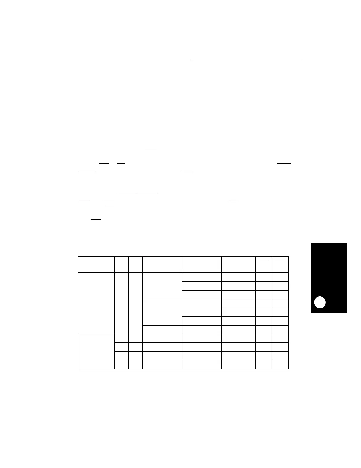
Table 17-1. Card Enable as Driven by the MPC823e
PRS
FIELD
A22 A23 PORT
SIZE
ACCESS
SIZE
MPC823e: A31
(SLOT: A0)
CE2
CE1
PRS
≠
‘110’
X X 8 bits 16 bit (only even) 0 1 0
8 bit odd 1 1 0
8 bits even 0 1 0
16 bits 16 bit (only even) 0 0 0
8 bit odd 1 0 1
8 bits even 0 1 0
No access X 1 1
PRS = ‘110’ 0 0 X X X 0 0
01 X X X 0 1
10 X X X 1 0
11 X X X 1 1