xii List of Figures
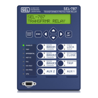
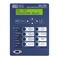
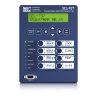
SEL-787 Relay Instruction Manual Date Code 20081022
Figure 4.8 Example 1 for WnCTC Selection.............................................................................................4.18
Figure 4.9 Example 2 for WnCTC Selection.............................................................................................4.20
Figure 4.10 REF Enable Logic....................................................................................................................4.27
Figure 4.11 REF Directional Element.........................................................................................................4.28
Figure 4.12 REF Protection Output (Extremely Inverse-Time O/C)...........................................................4.29
Figure 4.13 REF Function, REF1POL Setting Guide .................................................................................4.30
Figure 4.14 Instantaneous Overcurrent Element Logic...............................................................................4.32
Figure 4.15 Maximum Phase Time-Overcurrent Elements 51P1T and 51P2T ...........................................4.34
Figure 4.16 Residual Time-Overcurrent Elements 51G1T and 51G2T.......................................................4.35
Figure 4.17 Negative-Sequence Time-Overcurrent Element 51Q1T and 51Q2T ....................................... 4.36
Figure 4.18 Neutral Time-Overcurrent Elements 51N1T and 51N2T.........................................................4.37
Figure 4.19 U.S. Moderately Inverse Curve: U1.........................................................................................4.39
Figure 4.20 U.S. Inverse Curve: U2 ............................................................................................................4.40
Figure 4.21 U.S. Very Inverse Curve: U3.................................................................................................... 4.41
Figure 4.22 U.S. Extremely Inverse Curve: U4 ..........................................................................................4.42
Figure 4.23 U.S. Short-Time Inverse Curve: U5.........................................................................................4.43
Figure 4.24 I.E.C. Class A Curve (Standard Inverse): C1...........................................................................4.44
Figure 4.25 I.E.C. Class B Curve (Very Inverse): C2 .................................................................................4.45
Figure 4.26 I.E.C. Class C Curve (Extremely Inverse): C3 ........................................................................4.46
Figure 4.27 I.E.C. Long-Time Inverse Curve: C4 .......................................................................................4.47
Figure 4.28 I.E.C. Short-Time Inverse Curve: C5.......................................................................................4.48
Figure 4.29 Undervoltage Element Logic ...................................................................................................4.52
Figure 4.30 Overvoltage Element Logic...................................................................................................... 4.52
Figure 4.31 Overvoltage Element Logic...................................................................................................... 4.53
Figure 4.32 Dual-Level Volts/Hertz Time-Delay Characteristic 24CCS = DD .........................................4.54
Figure 4.33 Composite Inverse/Definite-Time Overexcitation Characteristic, 24CCS = ID ......................4.54
Figure 4.34 Volts/Hertz Inverse-Time Characteristic, 24IC = 0.5 ...............................................................4.57
Figure 4.35 Volts/Hertz Inverse-Time Characteristic, 24IC = 1 .................................................................. 4.57
Figure 4.36 Volts/Hertz Inverse-Time Characteristic, 24IC = 2 .................................................................. 4.58
Figure 4.37 Three-Phase Power Elements Logic ........................................................................................4.59
Figure 4.38 Power Elements Operation in the Real/Reactive Power Plane ................................................4.60
Figure 4.39 Over- and Underfrequency Element Logic ..............................................................................4.61
Figure 4.40 Loss-of-Potential (LOP) Logic ................................................................................................4.63
Figure 4.41 Demand Current Logic Outputs ...............................................................................................4.64
Figure 4.42 Response of Thermal and Rolling Demand Meters to a Step Input
(Setting DMTC = 15 minutes).............................................................................................4.65
Figure 4.43 Voltage V
S
Applied to Series RC Circuit.................................................................................4.66
Figure 4.44 Trip Logic ................................................................................................................................4.69
Figure 4.45 Close Logic ..............................................................................................................................4.71
Figure 4.46 Schematic Diagram of a Traditional Latching Device .............................................................4.72
Figure 4.47 Logic Diagram of a Latch Switch ............................................................................................4.73
Figure 4.48 SEL
OGIC Control Equation Variable/Timers SV01/SV01T—SV32T .....................................4.74
Figure 4.49 Result of Falling-Edge Operator on a Deasserting Input .........................................................4.77
Figure 4.50 Example Use of SEL
OGIC Variables/Timers............................................................................4.78
Figure 4.51 Counter 01 ................................................................................................................................4.79
Figure 4.52 Example of the Effects of the Input Precedence ......................................................................4.80
Figure 4.53 Phase Rotation Setting .............................................................................................................4.83
Figure 4.54 Breaker Failure Logic...............................................................................................................4.85
Figure 4.55 Analog Input Card Adaptive Name.......................................................................................... 4.85
Figure 4.56 Settings to Configure Input 1 as a 4–20 mA Transducer Measuring Temperatures
Between -50°C and 150°C ..................................................................................................4.88
Figure 4.57 Analog Output Number Allocation ..........................................................................................4.89
Figure 4.58 Analog Output Settings ............................................................................................................4.90
Figure 4.59 DC Mode Processing................................................................................................................4.90
Figure 4.60 AC Mode Processing................................................................................................................4.91