Lab 6: Analog-to-Digital Converter
TMS320F2837xD Microcontroller Workshop - Analog Subsystem 6 - 31
Build and Load
7. Click the “Build” button and watch the tools run in the Console window. Check for
errors in the Problems window.
8. Click the “Debug” button (green bug). A Launching Debug Session window will open.
Select only CPU1 to load the program on (i.e. uncheck CPU2), and then click OK. Then
the CCS Debug perspective view should open, the program will load automatically, and
you should now be at the start of main(). If the device has been power cycled since the
last lab exercise, be sure to configure the boot mode to EMU_BOOT_SARAM using the
Scripts menu.
Run the Code
9. In Main_6.c place the cursor in the “main loop” section, right click on the mouse key
and select Run To Line.
Open a memory browser to view some of the contents of the ADC results buffer. The
address label for the ADC results buffer is AdcBuf (type &AdcBuf) in the “Data” memory
page. Then <enter>
to view the contents of the ADC result buffer.
Note: Exercise care when connecting any jumper wires to the LaunchPad header pins
since the power to the USB connector is on!
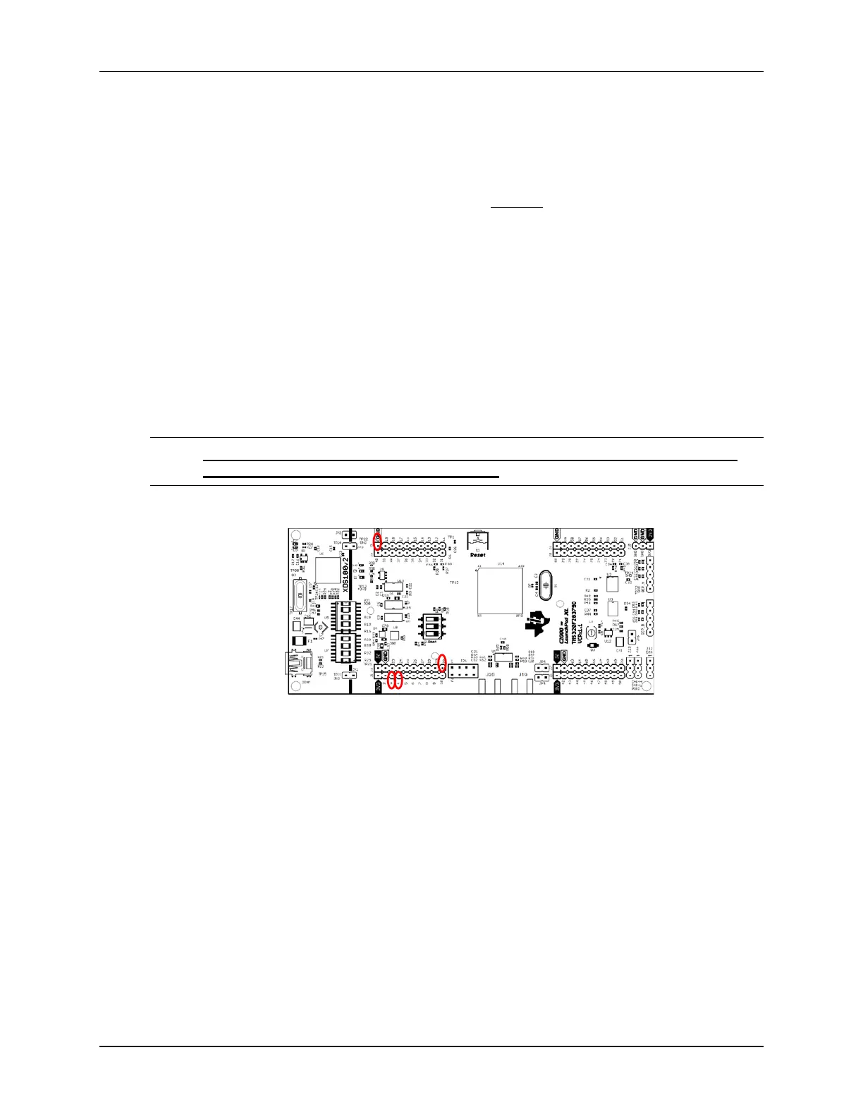
Refer to the following diagram for the location of the pins that will need to be connected:
10. Using a jumper wire, connect the ADCINA0 (header J3, pin #30) to “GND” (header J2,
pin #20) on the LaunchPad. Then run the code again, and halt it after a few seconds.
Verify that the ADC results buffer contains the expected value of ~0x0000. Note that you
may not get exactly 0x0000 if the device you are using has positive offset error.
11. Adjust the jumper wire to connect the ADCINA0 (header J3, pin #30) to “+3.3V”
(header J1, pin #3; GPIO-19) on the LaunchPad. (Note: pin # GPIO-19 has been set
to “1” in Gpio.c). Then run the code again, and halt it after a few seconds. Verify that
the ADC results buffer contains the expected value of ~0x0FFF. Note that you may
not get exactly 0x0FFF if the device you are using has negative offset error.
12. Adjust the jumper wire to connect the ADCINA0 (header J3, pin #30) to GPIO18 (header
J1, pin #4) on the LaunchPad. Then run the code again, and halt it after a few seconds.
Examine the contents of the ADC results buffer (the contents should be alternating
~0x0000 and ~0x0FFF values). Are the contents what you expected?
13. Open and setup a graph to plot a 50-point window of the ADC results buffer.
Click: Tools Graph Single Time and set the following values:

 Loading...


