Interrupts
TMS320F2837xD Microcontroller Workshop - Reset and Interrupts 4 - 15
interrupt lines (INT1 through INT12) are used to service the peripheral interrupts. A Peripheral
Interrupt Expansion (PIE) module multiplexes up to sixteen peripheral interrupts into each of the
twelve CPU interrupt lines, further expanding support for up to 192 peripheral interrupt signals.
The PIE module also expands the interrupt vector table, allowing each unique interrupt signal to
have its own interrupt service routine (ISR), permitting the CPU to support a large number of
peripherals.
The PIE module has an individual flag and enable bit for each peripheral interrupt signal. Each of
the sixteen peripheral interrupt signals that are multiplexed into a single CPU interrupt line is
referred to as a “group”, so the PIE module consists of 12 groups. Each PIE group has a 16-bit
flag register (PIEIFRx), a 16-bit enable register (PIEIERx), and a bit field in the PIE acknowledge
register (PIEACK) which acts as a common interrupt mask for the entire group. For a peripheral
interrupt to propagate to the CPU, the appropriate PIEIFR must be set, the PIEIER enabled, the
CPU IFR set, the IER enabled, and the INTM enabled. Note that some peripherals can have
multiple events trigger the same interrupt signal, and the cause of the interrupt can be determined
by reading the peripheral’s status register.
We have already discussed the interrupt process in the core. Now we need to look at the
peripheral interrupt expansion block. This block is connected to the core interrupt lines 1 through
12. The PIE block consists of 12 groups. Within each group, there are sixteen interrupt sources.
Each group has a PIE interrupt enable register and a PIE interrupt flag register. Note that
interrupt lines 13, 14, and NMI bypass the PIE block.
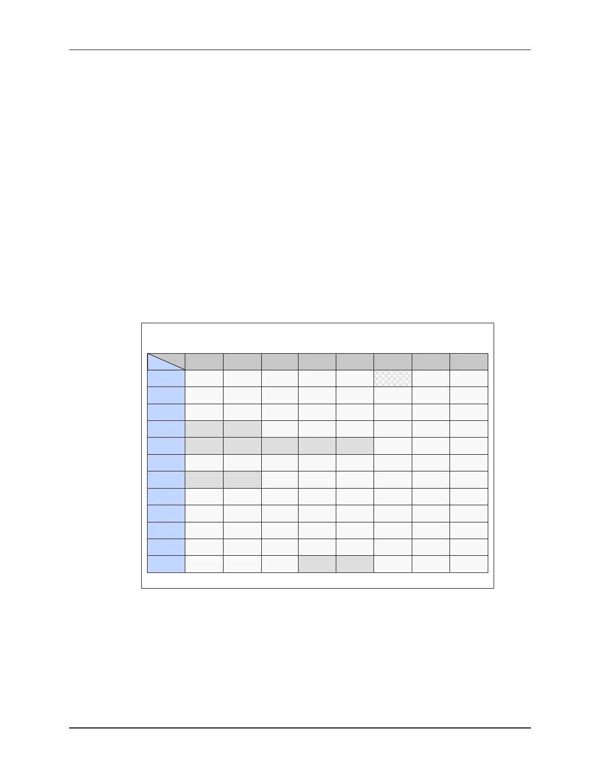
F2837xD PIE Assignment Table - Lower
INTx.8 INTx.7 INTx.6 INTx.5 INTx.4 INTx.3 INTx.2 INTx.1
INT1
WAKE TINT0 ADCD1 XINT2 XINT1 ADCC1 ADCB1 ADCA1
INT2
PWM8_
TZ
PWM7_
TZ
PWM6_
TZ
PWM5_
TZ
PWM4_
TZ
PWM3_
TZ
PWM2_
TZ
PWM1_
TZ
INT3
PWM8 PWM7 PWM6 PWM5 PWM4 PWM3 PWM2 PWM1
INT4
ECAP6 ECAP5 ECAP4 ECAP3 ECAP2 ECAP1
INT5
EQEP3 EQEP2
EQEP1
INT6
MCBSP
B_TX
MCBSP
B_RX
MCBSP
A_TX
MCBSP
A_RX
SPIB_TX SPIB_RX SPIA_TX SPIA_RX
INT7
DMA_CH6 DMA_CH5 DMA_CH4 DMA_CH3 DMA_CH2 DMA_CH1
INT8
SCID_TX SCID_RX SCIC_TX SCIC_RX
I2CB_
FIFO
I2CB
I2CA_
FIFO
I2CA
INT9
CANB_2 CANB_1 CANA_2 CANA_1 SCIB_TX SCIB_RX SCIA_TX SCIA_RX
INT10
ADCB4 ADCB3 ADCB2
ADCB_
EVT
ADCA4 ADCA3 ADCA2
ADCA_
EVT
INT11
CLA1_8 CLA1_7 CLA1_6 CLA1_5 CLA1_4 CLA1_3 CLA1_2 CLA1_1
INT12
FPU_UF FPU_OF VCU XINT5 XINT4 XINT3
The PIE assignment table maps each peripheral interrupt to the unique vector location for that
interrupt service routine. Notice the interrupt numbers on the left represent the twelve core group
interrupt lines and the interrupt numbers across the top represent the lower eight of the sixteen
peripheral interrupts within the core group interrupt line. The next figure shows the upper eight of
the sixteen peripheral interrupts within the core group interrupt line.

 Loading...


