Interrupts
4 - 16 TMS320F2837xD Microcontroller Workshop - Reset and Interrupts
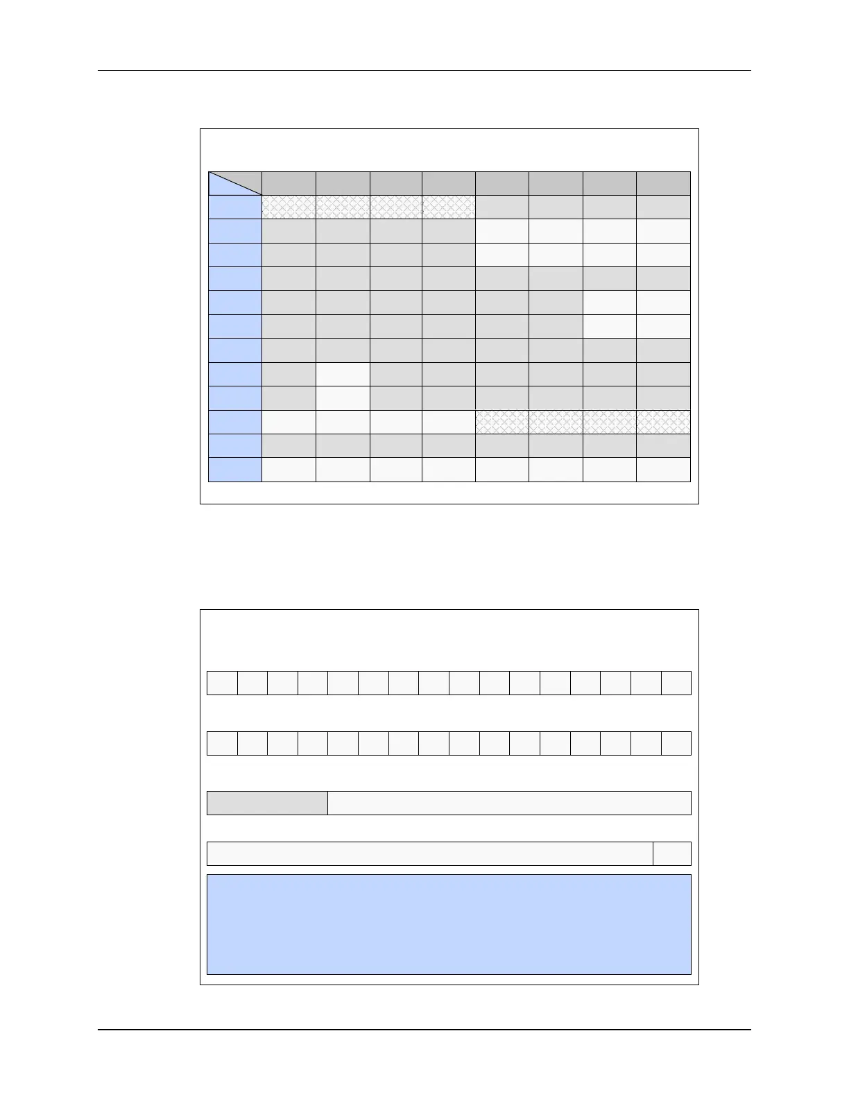
F2837xD PIE Assignment Table - Upper
INTx.16 INTx.15 INTx.14
INTx.13 INTx.12 INTx.11
INTx.10 INTx.9
INT1
IPC3 IPC2 IPC1 IPC0
INT2
PWM12_
TZ
PWM11_
TZ
PWM10_
TZ
PWM9_
TZ
INT3
EPWM12 EPWM11
EPWM10 EPWM9
INT4
INT5
SD2 SD1
INT6
SPIC_TX
SPIC_RX
INT7
INT8
UPPA
INT9
USBA
INT10
ADCD4
ADCD3 ADCD2
ADCD_
EVT
ADCC4
ADCC3 ADCC2
ADCC_
EVT
INT11
INT12
CLA_UF
CLA_OF
AUX_PLL
_SLIP
SYS_PLL
_SLIP
RAM_ACC
_VIOLAT
FLASH_C
_ERROR
RAM_C_
ERROR
EMIF_
ERROR
Similar to the core interrupt process, the PIE module has an individual flag and enable bit for
each peripheral interrupt signal. Each PIE group has a 16-bit flag register, a 16-bit enable
register, and a bit field in the PIE acknowledge register which acts as a common interrupt mask
for the entire group. The enable PIE bit in the PIECTRL register is used to activate the PIE
module.
PIE Registers
PIEVECT ENPIE
PIECTRL register
0
15 - 1
#include “F2837x_Device.h”
PieCtrlRegs.PIEIFR1.bit.INTx4 = 1; //manually set IFR for XINT1 in PIE group 1
PieCtrlRegs.PIEIER3.bit.INTx2 = 1; //enable PWM2 interrupt in PIE group 3
PieCtrlRegs.PIEACK.all = 0x0004; //acknowledge the PIE group 3
PieCtrlRegs.PIECTRL.bit.ENPIE = 1; //enable the PIE
PIEIFRx register (x = 1 to 12)
INTx.16 INTx.15 INTx.14 INTx.13 INTx.12 INTx.11 INTx.10
INTx.9
INTx.8 INTx.7 INTx.6 INTx.5 INTx.4 INTx.3
INTx.2 INTx.1
15 14 13 12 11 10 9 8 7 6 5 4 3 2 1 0
PIEIERx register (x = 1 to 12)
INTx.16 INTx.15 INTx.14 INTx.13 INTx.12 INTx.11 INTx.10 INTx.9 INTx.8 INTx.7 INTx.6 INTx.5 INTx.4 INTx.3 INTx.2 INTx.1
15 14 13 12 11 10 9 8 7 6 5 4 3 2 1 0
reserved PIEACKx
PIE Interrupt Acknowledge Register (PIEACK)
15 - 12 11 10 9 8 7 6 5 4 3 2 1 0

 Loading...


