LDI Intellectual Property.
Not for secondary distribution or replication, in part or entirety.
DIGISONDE-4D
SYSTEM MANUAL
VERSION 1.2.11
4-14 SECTION 4 – HARDWARE DESCRIPTION
4:23. The input data on port A[15..0] are converted to a complex input format (I and Q samples) in the
receive input formatter (RINF). In this common configuration, each down-conversion channel demodulates
the sampled data down to the baseband, then performs a low-pass filter operation, reduces the signal rate
(decimation), and outputs I and Q baseband data. The mixer stage provides the receive input channel selector
(RSEL), digital oscillator (NCO), and complex mixing logic (mixer) to translate the input data down to the
baseband. After the mixer, the 5-stage cascade integrator comb (CIC) is used for filtering and decimation.
After the CIC complex filter, the programmable finite impulse response (PFIR) filter provides CIC correc-
tion, spectral shaping, and further decimation.
4:24. A microcontroller (Figure 4-8) provides the bi-directional interface between the Control Platform
and the receiver to arrange automatic gain control and appropriate frequency selection. The transmitter-
generated B-Clock clears the receiver phases to zero in order to synchronize its operation with the transmit-
ter.
Digital Receiver Board
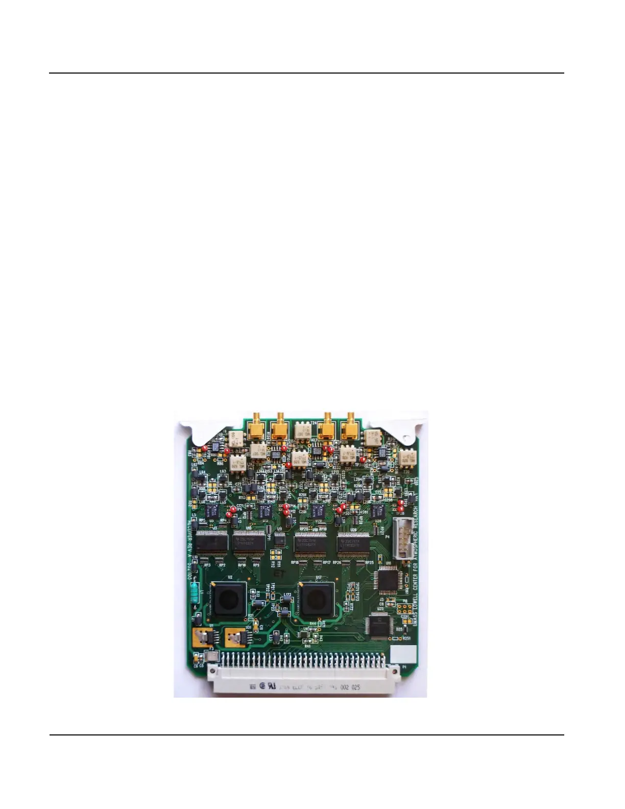
4:25. Figure 4-10 shows the front side of the Digital Receiver card. The four coaxial connectors on top of
the card feed four input signals to the receiver circuits. The digital output signals are fed through the 96-pin
DIN connector to the Preprocessor card. Each of the four inputs to the receiver card is transformer coupled to
a low-noise push-pull amplifier AD8008. The amplifier outputs are transformer coupled to the digitally con-
trolled variable gain amplifier (CLC5526), followed by a symmetric driver (THS4503) of the 16-bit ADC
(LTC2205) (Figure 4-8). The ADCs feed two GC 5016 Graychips (total of 8 receiving channels). Eight re-
ceiving channels are provided in this design for possible future expansion to twin frequency transmission.
Figure 4-10: Digital receiver PCB
 Loading...