LDI Intellectual Property.
Not for secondary distribution or replication, in part or entirety.
DIGISONDE-4D
SYSTEM MANUAL
VERSION 1.2.11
6-30 SECTION 6 - MAINTENANCE
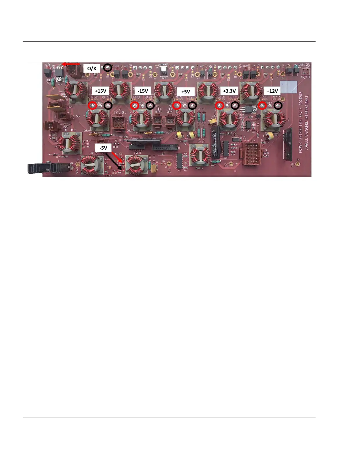
Figure 6-25: Power Distribution Card Showing Locations to Measure Output Voltages
TROUBLESHOOTING THE RF POWER AMPLIFIER MODULE
Special Test Equipment: 100MHz Oscilloscope
Reference Documents: RF Power Amplifier Schematics
6:96. The RF Amplifier card comprises two independent (referred to below as the two channels), three stage
wideband amplifiers. The entire 10 inch x 6 inch board is mounted to a 10 inch by 6 inch heat sink. The input
voltage is the system’s primary power of 25 to 28VDC, from the power supply via the power interface box
which contains FET switches.. The primary power is applied at the output end of the AMP board where it feeds
power to the 250V output stages. It is also routed back off the board to a twisted pair which runs down the un-
derside (the fin side) of the heat sink to feed power to the small signal end of the board. Keeping this twisted
pair on the back side of the AMP heat sink reduces coupling between output and input, thus reducing the danger
of a positive feedback situation.
6:97. The input signal to each amplifier channel is 1.7Vp-p, falling off slightly at the higher frequencies. The
input cable is terminated in a PI attenuator made up of a 68, 330 (or 220 in later production), and 68 ohm resis-
tors where the 330 (or 220) ohm resistor is bypassed by a 47pF (or 68 pf) capacitor to boost up the high fre-
quency output. The input signal is amplified to 12-14V by A1/A2 (36dB gain 500kHz to 500MHz amplifier
modules), which can be probed at the input of T7/T15. As a quick check, the output of T9/17 can be probed at
the input of the series resistors R124/126 or R204/206. There should be 20-25Vp-p at this point. Then the out-
put voltage 240-300Vp-p can be probed at the vertical wire connection (from T13/T21 to the PC board trace) at
the output of T13/T21.
6:98. The critical setting in the RF AMP is the bias voltage set by R67/147 for the input stages and R107/187
for the output stages. This bias voltage is pulsed, rising when the R BNC signal (Xmtr On from the front panel
input from the upper chassis) rises. The R BNC, via U41 and Q52/53 also applies the regulated +18V to ampli-
fiers A1 and A2. For waveform 1 this is 750usec every 5, or 10msec, so the bias voltage level can only be
measured by probing it with an oscilloscope. The bias voltage should be set to draw 2 to 4A idle current for the
input stages U8 and U16, and 0.75 to 1.5A for the output stage, U12 and U20, when no input signal is applied