LDI Intellectual Property.
Not for secondary distribution or replication, in part or entirety.
DIGISONDE-4D
SYSTEM MANUAL
VERSION 1.2.11
SECTION 4 – HARDWARE DESCRIPTION 4-21
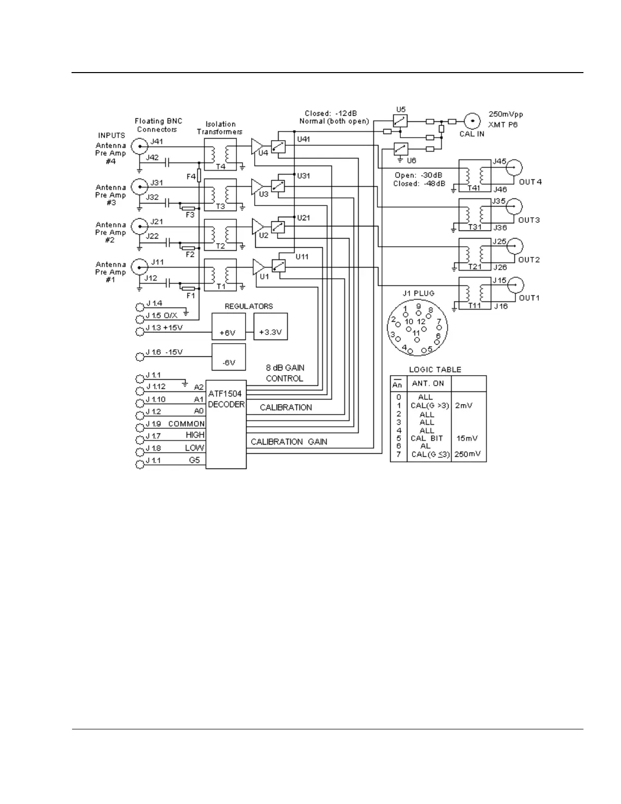
Figure 4-17: Antenna Switch Block Diagram
4:36. The input comes via short wires from BNC connectors mounted on the rear of the Antenna Switch’s
RF shielded enclosure. The four inputs are fed through transformers T1-T4, then through op amps U1-U4
into analog switches U11, U21, U31, and U41. The second input to the switches is a calibration signal gen-
erated on the Transmitter Card. The choice of switching between the antenna inputs and calibration signal is
software controlled by the CAL command on the J1 plug to the switchbox. The calibration signal level is
dependent on the gain setting selected by the user in the DCART menu. The software configures switches U5
and U6 to attenuate the level. The four outputs of the antenna switch, either antenna signals or calibration
signals, are fed out of the switchbox on SMB connectors, into the top of the (four) Tracker Card(s).
4:37. Every amplifier U1, U2, U3, U4 has a programmable gain control for signals from antennas using
switches U11, U21, U31, U41 accordingly. The decoder can set two gains with 9 dB difference.
4:38. The decoder is based on flash memory and can be reprogrammed on-board using the 10-pin JTAG
connector J3.


 To Next Page