LDI Intellectual Property.
Not for secondary distribution or replication, in part or entirety.
DIGISONDE-4D
SYSTEM MANUAL
VERSION 1.2.11
SECTION 4 – HARDWARE DESCRIPTION 4-25
RF POWER AMPLIFIER CHASSIS
4:47. The RF Amplifier consists of the aluminum chassis drawer, a power relay (24V solenoid) for switch-
ing the (approx) +27.5V input from the power supply. The power relay is controlled by the front panel switch
and by an FET on the RF Amp card which is commanded by input from the upper chassis via the RF Amp IO
connector. The chassis also houses the dual channel RF Power Amplifier card, with two independent ampli-
fiers both capable of 150W output, and the two Half-Octave Filter (HOF) cards. The chassis front panel
green LED displays the presence of primary power to the cards, and the two amber LED’s indicate the pres-
ence of transmitted power being output to the antennas from each of the two independent amplifiers located
on the RF Amplifier card.
RF Amplifier Card
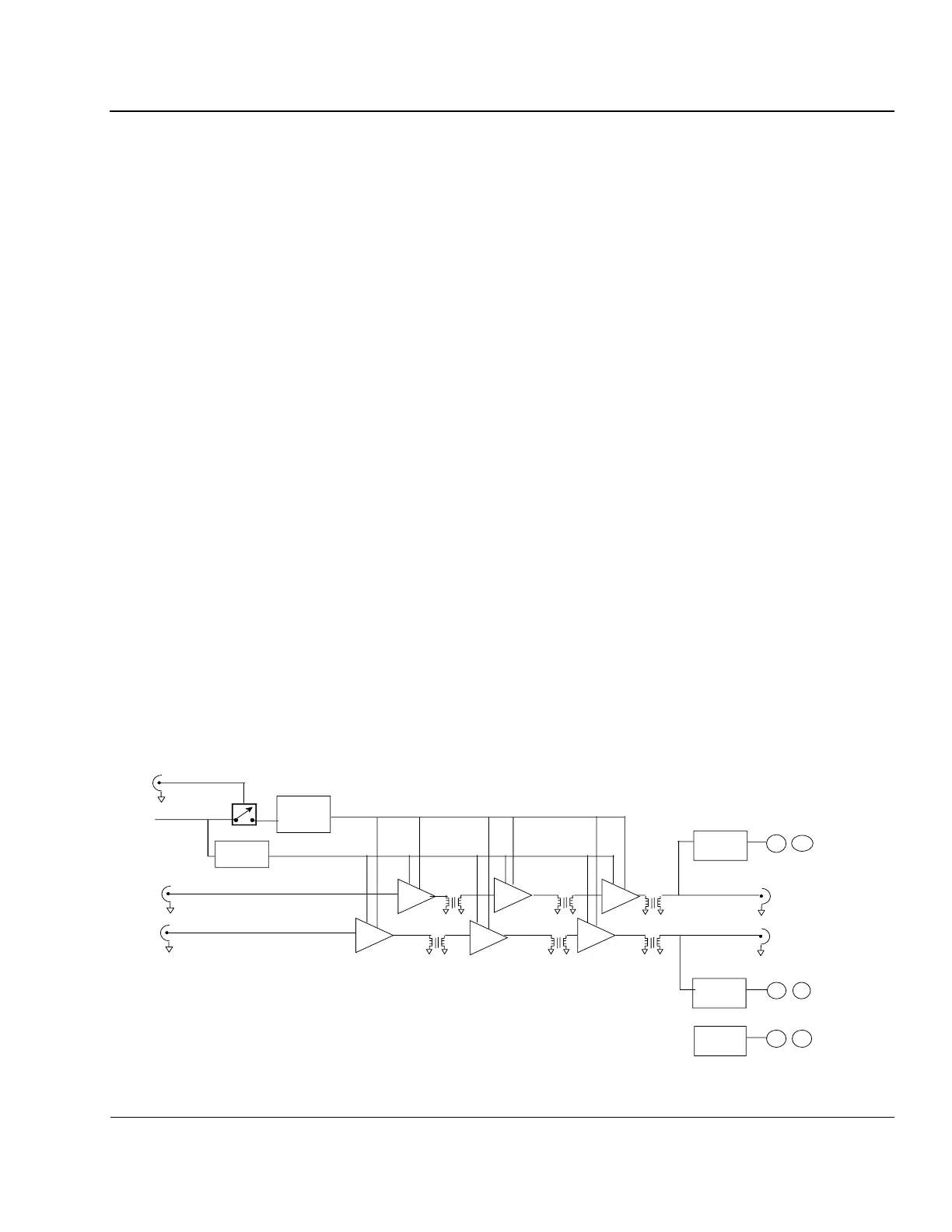
4:48. The RF Amplifier is comprised of two independent wideband amplifiers (referred to below as the
two channels) consisting of three stages, two drivers and a final (see Figure 4-23). The input signal to each
amplifier channel is 1.4Vp-p, falling off slightly at the higher frequencies. Each input stage (comprised of a
Motorola hybrid module) amplifies 10mW up to 0.5W. The output of the second stage is 20W (40Vp-p
across 22 ohms at the input to the final) and the output of the final stage is 150W. The entire 10 inch x 6 inch
board is mounted to a 10 inch by 6 inch heat sink. The input voltage is the system’s primary power of 25 to
28VDC. This input voltage is protected through a 8A fuse (not shown on the block diagram) at the input of
the 25 to 28V DC to the board. The primary power is applied at the output end of the amp board where it
feeds power, via the center tap on the primary of the 1:6 wideband transformers, to the 250Vpp output stag-
es. It is also routed back off the board to a twisted pair which runs down the underside (the fin side) of the
heatsink to feed power to the small signal end of the board. Keeping this twisted pair on the back side of the
AMP heat sink reduces coupling between output RF and input power, thus reducing the danger of a positive
feedback situation (i.e. oscillation).
Figure 4-21: RF AMP Block Diagram
4:49. The critical setting in the RF AMP is the bias voltage set by R67/147 for the input stages and
R107/187 for the output stages. The bias voltage is pulsed, rising when the R BNC signal (Xmtr On from the
regulated front panel input from the upper chassis) rises. The R BNC, via U41 and Q52/53 also applies the
regulated +18V to amplifiers A1 and A2. The turn-on voltage for various batches of MRF-141G MOSFET
P3
INPUTS
OUTPUTS
P2
P3
AMP
Envelope Detector
BIT
XMTR1
XMTR2
XMTR O N
P1
P2
BI AS V OLTAGE
LE V E L
AD JUS T
+2 4 VDC
MHW-592
MRF-1 41 G
MRF-1 41 G
Envelope
Detector
BIT
12
14
11
9
Thermal
Sensor
BIT
18
5
XMTR1
XMTR2
AMP
AMP
AMP
AMP
AMP
MOSF ET
Vo lt Reg