LCD Controller
MOTOROLA MPC823e REFERENCE MANUAL 18-27
LCD CONTROLLER
18
18.4.4 LCD Frame Buffer A Start Address Register
The 32-bit LCD frame buffer A start address (LCFAA) register contains the start address of
the frame buffer data that you want to send to your LCD panel. FIFO A is the destination for
your frame buffer data. For single-scan panels, FIFO A concatenated with FIFO B is used
to transfer data, so only the LCFAA register needs to be loaded. The DMA controller uses
the buffer start address to initiate data transfers from display memory, which can be system
memory or a dedicated display memory block. Because all LCD controller DMA bursts must
be 16-byte aligned, the four least-significant bits of the address are not used. This register
is read by the LCD controller at the start of each frame. Therefore, changing this register will
not take effect until the WBF bit expires.
FAA—FIFO A Address
This field designates the start address in display or system memory where LCD panel data
resides.
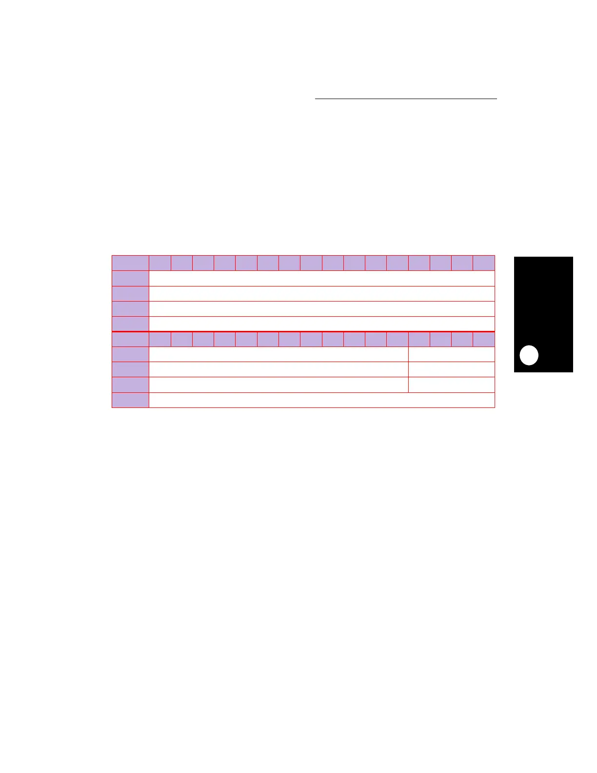
LCFAA
BIT 0 1 2 3 4 5 6 7 8 9 10 11 12 13 14 15
FIELD FAA
RESET —
R/W R/W
ADDR
IMMR & 0xFFFF0000 + 0x850
BIT 16 17 18 19 20 21 22 23 24 25 26 27 28 29 30 31
FIELD FAA X
RESET ——
R/W R/W R/W
ADDR
(IMMR & 0xFFFF0000) + 0x852
NOTE: X - “Don’t Care” and — = Undefined.
 Loading...

